NIST IR 1189 日本語訳
英語タイトル : Report of the Workshop on Estimation of Significant Advances in Computer Technology日本語タイトル : 計算機技術の重要な進歩の見積りに関するワークショップの報告書
公開日 : 1976-12-01
原文URL : https://csrc.nist.gov/pubs/ir/1189/final
翻訳編集 : 自動生成(有志による非公式の日本語訳), 原文取得日 : 2026-10-31, 訳文 : 239 / 240 ブロック
[要約] NIST IR 1189 は、1976 年 8 月 30 日と 31 日に米国標準局(NBS)で開かれた、計算機技術の重要な進歩の見積りに関するワークショップの報告書です。ワークショップには、産業界、研究機関、大学、他の政府機関の代表 20 名と計算機科学技術研究所(ICST)の職員が出席し、計算機技術の進歩に関する最新の科学技術情報を ICST に提供することを目的としていました。議論の焦点として、NBS が提案したデータ暗号化標準(DES)で暗号化されたデータの鍵を回復するための大規模なデジタルマシンの設計という具体的な問題が選ばれました。計算機アーキテクチャと半導体技術の進歩の見通しが発表され、鍵抽出マシンのいくつかの設計について、速度、規模、開発期間、費用などの見積りが作成されました。
NBSIR 76-1189
NBSIR 76-1189
Report of the Workshop on Estimation of Significant Advances in Computer Technology
計算機技術の重要な進歩の見積りに関するワークショップの報告書
Computer Systems Engineering Division
Institute for Computer Sciences and Technology
Washington, D. C. 20234
コンピュータシステム工学部門
計算機科学技術研究所(ICST)
Washington, D. C. 20234
December 1976
1976 年 12 月
U. S. DEPARTMENT OF COMMERCE
NATIONAL BUREAU OF STANDARDS
米国商務省
米国標準局(NBS)
NBSIR 76-1189
NBSIR 76-1189
REPORT OF THE WORKSHOP ON ESTIMATION OF SIGNIFICANT ADVANCES IN COMPUTER TECHNOLOGY
計算機技術の重要な進歩の見積りに関するワークショップの報告書
Edited by Paul Meissner
編集: Paul Meissner
Computer Systems Engineering Division
Institute for Computer Sciences and Technology
Washington, D. C. 20234
コンピュータシステム工学部門
計算機科学技術研究所(ICST)
Washington, D. C. 20234
December 1976
1976 年 12 月
A Report of the Workshop on Estimation of Significant Advances in Computer Technology
Held at the National Bureau of Standards
August 30-31, 1976
計算機技術の重要な進歩の見積りに関するワークショップの報告書
米国標準局(NBS)で開催
1976 年 8 月 30〜31 日
Edward Lohse, Chairman
Edward Lohse 議長
U.S. DEPARTMENT OF COMMERCE, Elliot L. Richardson, Secretary
Edward O. Vetter, Under Secretary
Dr. Betsy Ancker-Johnson, Assistant Secretary for Science and Technology
NATIONAL BUREAU OF STANDARDS, Ernest Ambler, Acting Director
米国商務省、Elliot L. Richardson、長官
Edward O. Vetter、次官
Dr. Betsy Ancker-Johnson、科学技術担当次官補
米国標準局(NBS)、Ernest Ambler、局長代行
1976 WORKSHOP ON ESTIMATION OF SIGNIFICANT ADVANCES IN COMPUTER TECHNOLOGY
計算機技術の重要な進歩の見積りに関する 1976 年ワークショップ
EXECUTIVE SUMMARY
エグゼクティブサマリー
The Institute for Computer Sciences and Technology has conducted a Workshop on Estimation of Significant Advances in Computer Technology. This Workshop was held at the National Bureau of Standards on August 30 - 31, 1976, and was attended by 20 representatives from industry, research organizations, universities, and other Government agencies, together with a number of ICST staff members.
計算機科学技術研究所(ICST)は、計算機技術の重要な進歩の見積りに関するワークショップを実施しました。このワークショップは、1976 年 8 月 30〜31 日に米国標準局(NBS)で開催され、産業界、研究機関、大学、その他の政府機関から 20 人の代表者と、ICST の職員数名が出席しました。
The Workshop was intended to provide ICST with current scientific and technical information on advances in computer technology which could significantly impact the Federal Government's knowledge and use of computer technology developments in relation to computer security and export administration.
このワークショップは、コンピュータセキュリティと輸出管理に関連して、連邦政府による計算機技術の進展の把握と利用に大きく影響しうる、計算機技術の進歩に関する最新の科学的・技術的情報を ICST に提供することを目的としていました。
In order to focus the attention of the Workshop, a specific problem was chosen, namely the design of a large-scale digital machine which could be used for recovering the key used for encrypting data under the proposed NBS Data Encryption Standard (DES).
ワークショップの焦点を絞るため、具体的な問題として、提案された NBS データ暗号化標準(DES)で暗号化されたデータの鍵を復元するために使える大規模なデジタルマシンの設計が選ばれました。
Presentations were made on the anticipated advances in computer architecture and in semiconductor technology. It was indicated that the present trends in component density for LSI, which has been increasing exponentially since the late 1960's, will continue in the same manner for at least the next five years. The density for logic circuitry is expected to grow from about 3000 gates per chip in 1975 to about 250,000 gates per chip in 1981; in memory chips the density will increase from about 25,000 bits per chip to about 1,000,000 bits per chip. The speed of logic circuitry has been increasing by about 1.5 megahertz per year for some ten years, which a speed of 30 megahertz being achievable at the present time. Speed-power ratios have been improving by a factor of 10 about every four years and a similar improvement appears likely in the next four years. The highest performance appears to be attainable with complementary metal-oxide-semiconductor, silicon-on-sapphire (CMOS-SOS) technology. This technology offers a speed-power product of one to two picojoules and a speed of 30 megahertz, and is expected to be reasonably available by 1981.
計算機アーキテクチャと半導体技術について、見込まれる進歩に関する発表が行われました。1960 年代後半から指数関数的に増加してきた LSI の部品密度の現在の傾向は、少なくとも今後 5 年間は同じように続くと示されました。論理回路の密度は、1975 年の 1 チップあたり約 3,000 ゲートから、1981 年には 1 チップあたり約 250,000 ゲートに増加すると見込まれ、メモリチップの密度は、1 チップあたり約 25,000 ビットから約 1,000,000 ビットに増加します。論理回路の速度は約 10 年間、毎年約 1.5 メガヘルツずつ向上しており、現在は 30 メガヘルツの速度が達成可能です。速度対電力比は約 4 年ごとに 10 倍ずつ改善されており、今後 4 年間も同様の改善が見込まれます。最高の性能は、相補型金属酸化膜半導体・サファイア上シリコン(CMOS-SOS)技術で達成可能と思われます。この技術は、1〜2 ピコジュールの速度・電力積と 30 メガヘルツの速度を提供し、1981 年までには十分に入手可能になると見込まれています。
Semiconductor sources are presently concentrating on achieving high density at low cost, with less emphasis on extending high speed performance at the upper limits. Large production volumes are required in order to realize the most favorably prices, and this volume requirement is a barrier to many low-volume applications, including those of the military. A single order for one million chips would not be considered large.
半導体の供給元は、現在、低費用で高密度を達成することに集中しており、上限での高速性能の拡張にはあまり重点を置いていません。最も有利な価格を実現するには大量の生産量が必要であり、この量の要件は、軍事用途を含む多くの少量用途にとって障壁となっています。100 万チップの単一の注文であっても、大口とはみなされません。
Several designs were formulated for key-extraction machines for the data encrypted under the DES, and estimates were developed for the speed, size, development time, cost, and other factors. It is significant to note that while the technological factors for such a development are separately available (such as high density, high speed, low power, and low cost) these factors are not presently attainable in combined form as would be required for a successful key extraction machine. Rather, the various factors tend to be mutually exclusive, and extensive development effort and time will be required before all the factors become realizable in any one production device. To achieve a key exhaustion time on the order of one day, it was estimated that the cost would be several tens of millions of dollars, and that such a machine could not be placed in operation before 1990.
DES で暗号化されたデータの鍵抽出マシンについて、いくつかの設計が定式化され、速度、規模、開発期間、費用、その他の要因の見積りが作成されました。そのような開発に必要な技術的要因は(高密度、高速、低消費電力、低費用など)個別には利用可能であるものの、鍵抽出マシンの成功に求められるように、これらの要因を組み合わせた形で達成することは現時点ではできないという点が重要です。むしろ、さまざまな要因は互いに両立しない傾向があり、すべての要因が 1 つの製品デバイスで実現可能になるまでには、大規模な開発の取組みと時間が必要になります。鍵の全数探索時間を 1 日程度にするには、費用は数千万ドルになり、そのようなマシンは 1990 年より前には運用に入れられないと見積もられました。
TABLE OF CONTENTS
目次
APPENDICES
付録
A. LIST OF WORKSHOP ATTENDEES
A. ワークショップ出席者の一覧
REPORT OF THE 1976 WORKSHOP ON ESTIMATION OF SIGNIFICANT ADVANCES IN COMPUTER TECHNOLOGY
計算機技術の重要な進歩の見積りに関する 1976 年ワークショップの報告書
1. Introduction
1. はじめに
The Institute for Computer Sciences and Technology (ICST) of the National Bureau of Standards has responsibility under its basic charter, Public Law 89-306, to develop mandatory Federal Information Processing Standards, provide technical assistance and advice to Federal departments and agencies and conduct necessary research in computer sciences and technology. These objectives are accomplished through a comprehensive technical program that stresses high-priority national computer problems and issues. Specifically, ICST is responsible for monitoring advances in computer science and technology, assessing their technologically-derived impact and striving to promote their application and acceptance within the Federal Government.
米国標準局(NBS)の計算機科学技術研究所(ICST)は、その基本的な設立趣旨である公法 89-306 に基づき、強制力のある連邦情報処理標準を策定し、連邦の省庁と機関に技術的な支援と助言を提供し、計算機科学技術における必要な研究を実施する責任を負っています。これらの目標は、優先度の高い国家的なコンピュータの問題や課題に重点を置く包括的な技術プログラムによって達成されます。具体的には、ICST は、計算機科学技術の進歩を把握し、それらが技術面にもたらす影響を評価し、連邦政府内でのその応用と受け入れの促進に努める責任を負っています。
1.1 Purpose of the Workshop
1.1 ワークショップの目的
This Workshop was conducted at the National Bureau of Standards (NBS), Gaithersburg, Maryland, on August 30-31, 1976, to provide ICST with current scientific and technical information on advances in computer technology which could significantly impact the Federal Government's knowledge and use of these advances in relation to computer security and export administration.
このワークショップは、1976 年 8 月 30〜31 日に Maryland 州 Gaithersburg の米国標準局(NBS)で実施され、コンピュータセキュリティと輸出管理に関連して、連邦政府によるこれらの進歩の把握と利用に大きく影響しうる、計算機技術の進歩に関する最新の科学的・技術的情報を ICST に提供することを目的としていました。
The focus of the Workshop was on advances in the design, architecture and manufacturing of computer systems and related equipment which could be identified or estimated as characterizing the present state-of-the-art and the predictable future.
ワークショップの焦点は、計算機システムと関連機器の設計、アーキテクチャ、製造における進歩で、現在の最新技術水準と予測可能な将来を特徴づけるものとして特定または見積もることができるものに置かれました。
1.1.1 Computer Security
1.1.1 コンピュータセキュリティ
The subject areas of personal privacy, data confidentiality, and computer security are of the greatest National interest. The Privacy Act of 1974 (5 U.S.C. 552a) imposes numerous requirements upon Federal agencies to prevent the misuse of information about individuals and assure its integrity and security. ICST has been assigned certain responsibilities in the development of standards and guidelines for use by the Federal agencies in implementing the requirements of the Privacy Act and in complying with requirements for computer security and data integrity.
個人のプライバシー、データの機密性、コンピュータセキュリティという主題領域は、国家的に最大の関心事です。1974 年プライバシー法(5 U.S.C. 552a)は、個人に関する情報の悪用を防ぎ、その完全性とセキュリティを確保するために、連邦機関に多くの要件を課しています。ICST は、連邦機関がプライバシー法の要件を実施し、コンピュータセキュリティとデータの完全性の要件に準拠する際に使用する標準とガイドラインの策定について、一定の責任を課されています。
1.1.2 Export Administration
1.1.2 輸出管理
ICST has significant responsibilities in the area of export control to maintain an awareness of current and projected computer technology, production capability, and usage. This knowledge and expertise is made available for use within the Federal Government in the determination of export control criteria and parameters for various classes of ADP equipment.
ICST は、現在および将来の計算機技術、生産能力、利用状況の把握を維持するという、輸出管理の分野における重要な責任を負っています。この知識と専門知識は、さまざまな種類の ADP 機器に対する輸出管理の基準とパラメータを決定する際に、連邦政府内で利用できるようにされています。
1.2 Topic Selected as Computer Technology Vehicle
1.2 計算機技術の媒体として選ばれた題材
In order to achieve the objectives of the Workshop, a specific topic was addressed as a useful vehicle for examining current and projected capabilities for the design and manufacture of computer systems and related hardware. Consideration of this topic also provided direct and immediate assistance to NBS in the development of standards and guidelines, especially those related to computer security.
ワークショップの目標を達成するため、計算機システムと関連ハードウェアの設計・製造における現在および将来の能力を調べる有用な媒体として、具体的な題材が取り上げられました。この題材の検討は、NBS が標準とガイドライン、とくにコンピュータセキュリティに関するものを策定する際にも、直接的かつ即時の助けとなりました。
The selected topic was representative of a class of problems whose performance was not assumed to be constrained by traditional computer architectures and techniques. The topic involved the design and fabrication of a system to recover the key used to encrypt data under the NBS-proposed Data Encryption Standard (DES). (See Appendix B.)
選ばれた題材は、性能が従来の計算機アーキテクチャや技術に制約されるとは想定されない、ある種の問題の代表例でした。この題材は、NBS が提案したデータ暗号化標準(DES)で暗号化されたデータの鍵を復元するシステムの設計と製作に関するものです(付録 B を参照)。
1.3 Expected Significance of Results
1.3 結果に期待される意義
ICST will use the information from the Workshop to (1) estimate the computer resources necessary to recover a key used in any particular instance by the proposed DES, (2) model advanced computer systems for which computer security safeguards must be emplaced to prevent computer fraud and to meet legislated privacy requirements, and (3) assess the potential technical significance associated with the export of computer-related products and technology.
ICST は、ワークショップで得た情報を、(1) 提案された DES を用いて特定の事例で使われた鍵を復元するために必要な計算機資源の見積り、(2) コンピュータ詐欺を防ぎ、法制化されたプライバシー要件を満たすため、コンピュータセキュリティの保護対策を講じなければならない高度な計算機システムのモデル化、(3) 計算機関連の製品と技術の輸出に伴う潜在的な技術的意義の評価、に使用します。
1.3.1 Workshop Report
1.3.1 ワークショップの報告書
The product of the Workshop is this report containing technical information developed by the participants with regard to the topics considered. This report will serve as a significant element in the formulation of recommendations by NBS for use within the Executive Branch, and for submission to the Congress and to public groups for needed action pertaining to the subject areas of the Workshop. The report is intended as a factual summary of the Workshop for information purposes.
ワークショップの成果物は、検討した題材に関して参加者が作成した技術情報を含む本報告書です。この報告書は、行政府内で使用するための、また、ワークショップの主題領域に関して必要な対応のために議会や一般団体に提出するための、NBS の勧告を作成する際の重要な要素となります。報告書は、情報提供を目的として、ワークショップの事実に基づく要約とすることを意図しています。
1.4 Organization of the Workshop
1.4 ワークショップの構成
Technical experts representing a cross-section of the computer industry were brought together for the Workshop, representing the areas of semiconductor manufacturing, logic design, system architecture, and system fabrication. In preparation for the Workshop, announcements were sent to relevant associations and professional groups with the request that they identify suitable individuals who should be encouraged to attend the Workshop. The individuals so identified included representatives from industry, research laboratories, universities, consulting firms, and Government agencies. In addition, the Workshop was publicly announced to notify individuals wishing to contribute to the objectives of the Workshop. Several members of the ICST staff were present in order to contribute to the Workshop and to benefit from the available information. The Workshop was chaired by Mr. Edward Lohse, Director of Engineering - Operations, of the Burroughs Corporation.
ワークショップには、計算機産業の幅広い分野を代表する技術専門家が集められ、半導体製造、論理設計、システムアーキテクチャ、システム製作の分野を代表していました。ワークショップの準備として、関連する協会や専門家グループに案内が送られ、ワークショップへの出席を勧めるのに適した人物を特定するよう依頼しました。こうして特定された人々には、産業界、研究所、大学、コンサルティング会社、政府機関の代表者が含まれていました。さらに、ワークショップの目標に貢献したい人々に知らせるため、ワークショップは公に告知されました。ICST の職員数名が、ワークショップに貢献するとともに、得られる情報から利益を得るために出席しました。ワークショップの議長は、Burroughs Corporation の工学・運用部門ディレクターの Mr. Edward Lohse が務めました。
1.5 Opening Remarks
1.5 冒頭の挨拶
Workshop participants were welcomed by the conference chairman. Mr. Lohse described the purpose of the Workshop and identified the topic selected as a vehicle for exploring advances in computer technology, namely the design of a machine for extracting the key used in encrypting data under the NBS-proposed Data Encryption Standard.
ワークショップの参加者は、会議の議長に歓迎されました。Mr. Lohse は、ワークショップの目的を説明し、計算機技術の進歩を探る媒体として選ばれた題材、すなわち、NBS が提案したデータ暗号化標準でデータを暗号化する際に使われる鍵を抽出するマシンの設計を示しました。
In opening remarks, Dr. Ruth M. Davis, Director of ICST outlined the responsibilities of ICST and the expectations for the Workshop. Mr. John Diebold was identified as Honorary Chairman for this Workshop and a second workshop to be held on the mathematical aspects of the proposed encryption algorithm. Dr. Davis identified three of the main responsibilities of ICST as (1) keeping abreast of advances in computer technology, (2) furnishing advice and guidance to the Federal Government on the effective management and utilization of ADP, and (3) performing gap-filling research and development on the basis of recognized needs.
ICST 所長の Dr. Ruth M. Davis は、冒頭の挨拶で、ICST の責任とワークショップへの期待を概説しました。Mr. John Diebold は、このワークショップと、提案された暗号化アルゴリズムの数学的な側面に関する第 2 のワークショップの名誉議長として紹介されました。Dr. Davis は、ICST の主な責任のうち 3 つとして、(1) 計算機技術の進歩に遅れないこと、(2) ADP の効果的な管理と利用について連邦政府に助言と指針を提供すること、(3) 認識されたニーズに基づいて、空白を埋める研究開発を実施すること、を挙げました。
The process of establishing standards was depicted as becoming more intricate as the art of data processing advances and relationships become more complex; this is particularly evident in the area of interface standards. ICST was identified as the champion of sometimes unpopular (but important!) causes, having a special regard for the often-overlooked and lonely user. Current efforts to develop communications protocols for the library community were mentioned. The development of safeguards for computer systems was described, the intent being to lower the vulnerability to risks to the same extent that the utility has been increased.
標準を確立する過程は、データ処理の技術が進歩し、関係が複雑になるにつれて、より込み入ったものになると説明されました。これはとくにインタフェース標準の分野で顕著です。ICST は、見過ごされがちで孤立した利用者に特別な配慮を払いながら、ときに不人気な(しかし重要な)課題を擁護する存在であると位置づけられました。図書館コミュニティのための通信プロトコルを策定する現在の取組みにも言及がありました。コンピュータシステムの保護対策の開発も説明され、その意図は、有用性が高まったのと同じ程度に、リスクに対する脆弱性を低くすることにあるとされました。
Dr. Davis expressed the hope that this Workshop might identify the limits which will be encountered by our present computer technology so developers might proceed consciously toward these limits rather than stumbling across them.
Dr. Davis は、このワークショップによって、現在の計算機技術が直面する限界が明らかになり、開発者がそれらの限界につまずくのではなく、意識的に限界に向かって進めるようになることへの期待を述べました。
In the export area, ICST attempts to serve as a mediator between the business community and the security community. ADP is currently distinguished by exhibiting an increasing rate of increase in the international balance of trade.
輸出の分野で、ICST は、産業界とセキュリティ関係者の間の調停者として役立つよう努めています。現在、ADP は国際貿易収支における増加の速度が高まっているという特徴があります。
Commenting on the scenario selected for the Workshop, Dr. Davis pointed out that the selected topic involved a standard of general interest, and that it provided a view toward the future. It also involved a problem having no analytic solution.
Dr. Davis は、ワークショップのために選ばれたシナリオについて、選ばれた題材が一般的な関心を集める標準に関わるものであり、将来への展望を与えるものであると指摘しました。また、解析的な解法のない問題にも関わるものでした。
Dr. Davis announced that the second Workshop in this two-part series would deal with mathematical and statistical aspects of the selected topic and would be chaired by Mr. Julian Bigelow of the Institute for Advanced Study, Princeton, N.J.
Dr. Davis は、この 2 部構成のシリーズの第 2 のワークショップが、選ばれた題材の数学的・統計的な側面を扱い、New Jersey 州 Princeton の Institute for Advanced Study の Mr. Julian Bigelow が議長を務めることを発表しました。
2. Description of Topic Serving as Technology Case Study for the Workshop
2. ワークショップの技術的な事例研究となった題材の説明
The topic selected as a vehicle for consideration by the Workshop, namely a machine to extract the key used for encipering messages under the NBS-proposed Data Encryption Standard (DES), was put forth by Dr. Dennis Branstad of ICST. After describing the DES enciphering algorithm, he outlined the "worst-case" conditions for deriving a key using the known-plaintext threat. In this situation, it is assumed that an adversary has sufficient matching plaintext and cipertext, encrypted under a fixed, but unknown, key. He then presented an algorithm for extracting the key by exhaustion, first using a single machine, figure 1, and then using a parallel array of machines, figure 2. In the first case, figure 1, a block of plain text and a corresponding block of encrypted text are entered into an encryption test unit. The unit then encrypts the plain text under one key after another, each time comparing the result with the encrypted text input. If a match is obtained, the current value of the key is considered to be the desired answer and is printed out. If a match is not obtained, the value of the key is advanced by one and the process is repeated. The process would continue, if necessary, until all 256 values had been tested. In the case of the parallel machine, figure 2, a set of encryption test units would be employed, each functioning in the manner described above. Each unit would be assigned a portion of the key space over which to perform its testing. The machine would be supplied with a pair of blocks, one being plain text and the other being the encrypted version. The machine would operate until a match was obtained, or until the entire key space (256 values) was exhausted. By having n units operating in parallel, the search time can be reduced by a factor of n.
ワークショップが検討する媒体として選ばれた題材、すなわち、NBS が提案したデータ暗号化標準(DES)でメッセージを暗号化する際に使われる鍵を抽出するマシンは、ICST の Dr. Dennis Branstad が提示しました。DES の暗号化アルゴリズムを説明した後、彼は、既知平文攻撃を用いて鍵を導出する場合の「最悪ケース」の条件を概説しました。この状況では、敵対者が、固定された未知の鍵で暗号化された、十分な量の対応する平文と暗号文を持っていると想定します。次に彼は、全数探索によって鍵を抽出するアルゴリズムを、最初に単一のマシンを使う場合(図 1)、続いてマシンの並列アレイを使う場合(図 2)で示しました。最初の場合(図 1)では、平文の 1 ブロックと、それに対応する暗号文の 1 ブロックが、暗号化試験ユニットに入力されます。ユニットは、1 つずつ鍵を変えながら平文を暗号化し、そのたびに結果を入力された暗号文と比較します。一致が得られれば、その時点の鍵の値が求める答えとみなされ、印字されます。一致が得られなければ、鍵の値を 1 つ進めて、この過程を繰り返します。この過程は、必要であれば、256 個の値すべてが試されるまで続きます。並列マシンの場合(図 2)は、暗号化試験ユニットの集合が使われ、各ユニットは上記の方法で動作します。各ユニットには、試験を行う鍵空間の一部が割り当てられます。マシンには、平文である 1 つと、その暗号化されたもう 1 つの、2 つのブロックの組が与えられます。マシンは、一致が得られるか、鍵空間全体(256 個の値)が尽きるまで動作します。n 個のユニットを並列に動作させることで、探索時間を n 分の 1 に減らすことができます。
As to whether the correct key could always be extracted on the basis of a single pair of blocks, it was pointed out that the correctness of a tentative key could be quickly ascertained simply by testing it with another pair of blocks.
正しい鍵が、1 組のブロックだけで常に抽出できるかどうかについては、仮の鍵が正しいかどうかは、別のブロックの組で試すだけで、すぐに確認できると指摘されました。
It was proposed that the Workshop participants use their specialized knowledge to devise implementations embodying this extraction algorithm, making maximum use of the advanced technology expected to be available as far into the future as this could reasonably be projected. Factors of interest would be the architectures of such machines, the type of circuitry, speed of operation, reliability and maintainability, size, power, and cooling requirements.
ワークショップの参加者が、専門知識を使って、この抽出アルゴリズムを具体化する実装を考案し、合理的に予測できる限り先の将来に利用可能と見込まれる先進技術を最大限に活用することが提案されました。関心の対象となる要因は、そのようなマシンのアーキテクチャ、回路の種類、動作速度、信頼性と保守性、大きさ、電力、冷却の要件です。
Dr. Branstad was followed by Dana Grubb of ICST who reviewed the NBS implementation of the DES using small and medium scale integration and TTL logic, in order to acquaint the participants with the computational details and circuit considerations (see Figure 3). The NBS implementation, designed for performing practical tests rather than maximum speed, performs the algorithm in 8 microseconds and requires an additional 26 microseconds to load and unload data, which is done in eight 8-bit bytes. The basic operations are performed with 181 ICs; additional test logic bring this to 205 ICs, representing about 5000 gates. PROMs are used to implement the functions of the S-boxes. The encryption time for the NBS equipment could be reduced to about 3.4 microseconds using special shift registers. The use of Schottky TTL could bring this down to about 1.7 microseconds. In answer to a question, the speed of MECL 10K logic was stated to be about 5 nanoseconds per stage and that of Schottky TTL as about 3 nanoseconds. As a point of reference, the time to exhaust all possible keys (256) with the NBS equipment would by about 17,000 years.
Dr. Branstad に続いて、ICST の Dana Grubb が、小規模・中規模集積回路と TTL 論理を使った NBS の DES 実装を紹介し、参加者に計算の詳細と回路上の考慮事項を理解してもらいました(図 3 を参照)。この NBS の実装は、最大速度ではなく実用的な試験を行うために設計されたもので、アルゴリズムを 8 マイクロ秒で実行し、データのロードとアンロードにさらに 26 マイクロ秒を要します。データは 8 ビットのバイト 8 個で扱われます。基本的な演算は 181 個の IC で行われ、追加の試験用論理により 205 個の IC となり、約 5,000 ゲートに相当します。S ボックスの機能の実装には PROM が使われています。NBS の機器の暗号化時間は、特殊なシフトレジスタを使えば約 3.4 マイクロ秒に短縮できます。Schottky TTL を使えば、約 1.7 マイクロ秒まで短縮できます。質問への回答として、MECL 10K 論理の速度は 1 段あたり約 5 ナノ秒、Schottky TTL の速度は約 3 ナノ秒であると述べられました。参考までに、NBS の機器ですべての可能な鍵(256)を探索し尽くす時間は、約 17,000 年になります。
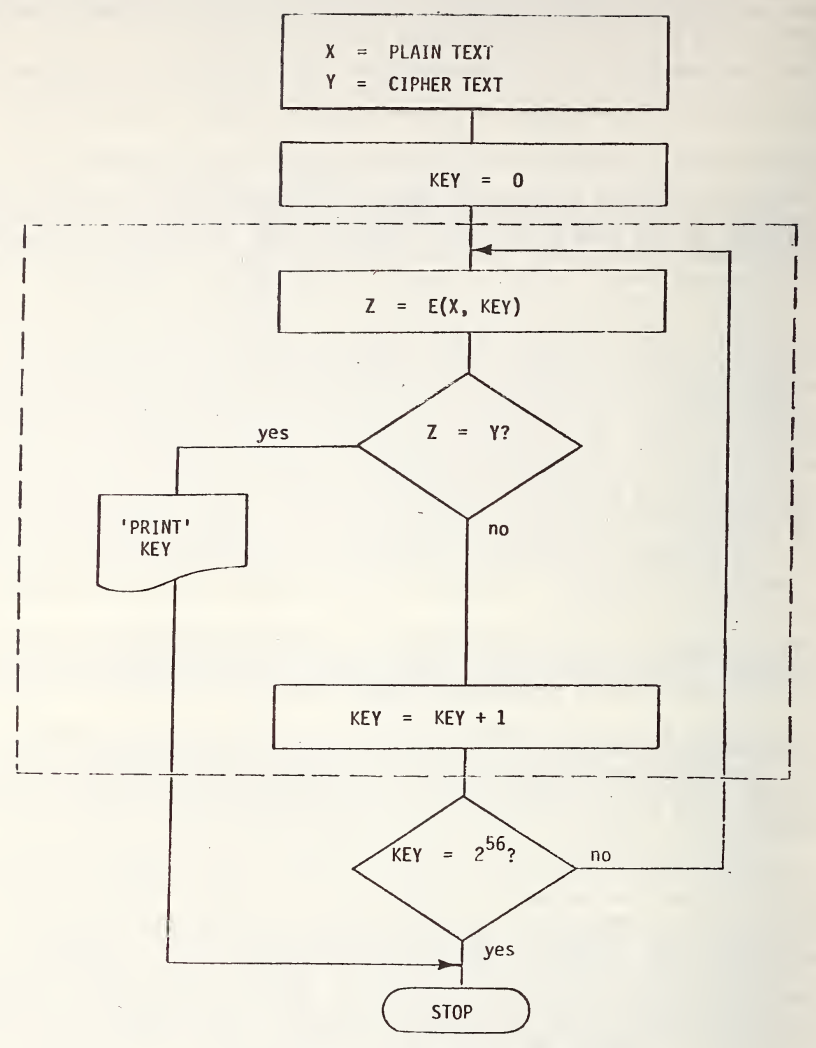
鍵抽出アルゴリズムの流れ図です。「X = PLAIN TEXT」と「Y = CIPHER TEXT」の箱の後に「KEY = 0」の箱があります。破線の枠の中には、「Z = E(X, KEY)」の箱と「Z = Y?」の判断があります。「yes」の場合は左側の出力記号「'PRINT' KEY」を経て「STOP」に進み、「no」の場合は「KEY = KEY + 1」の箱に進みます。破線枠の下には「KEY = 2^56?」の判断があります。「no」の場合は右側の線を通ってループの先頭(「Z = E(X, KEY)」の直前)に戻り、「yes」の場合は終端「STOP」に進みます。
FIGURE 1. KEY EXTRACTION ALGORITHM
図 1. 鍵抽出アルゴリズム
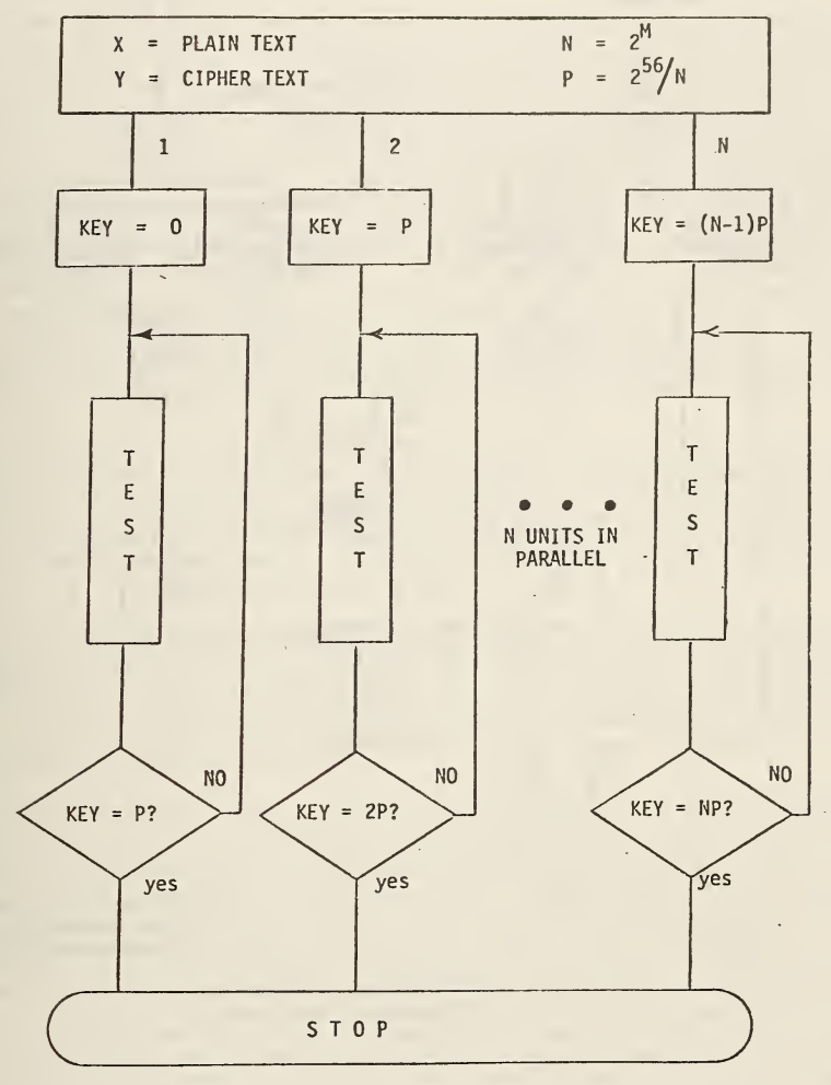
鍵抽出アルゴリズムの並列版の流れ図です。上の箱に「X = PLAIN TEXT」「Y = CIPHER TEXT」「N = 2^M」「P = 2^56/N」とあります。そこから「1」「2」「N」の 3 本の枝が下り、それぞれ「KEY = 0」「KEY = P」「KEY = (N-1)P」の箱、縦長の「TEST」の箱、判断(「KEY = P?」「KEY = 2P?」「KEY = NP?」)に進みます。「NO」は右側を通って TEST の上に戻り、「yes」は下へ進みます。2 本目と 3 本目の間に点 3 つと「N UNITS IN PARALLEL」(N 台を並列)の文字があります。すべての「yes」が下端の横長の端子「S T O P」に合流します。
FIGURE 2. PARALLEL VERSION OF KEY EXTRACTION ALGORITHM
図 2. 鍵抽出アルゴリズムの並列版
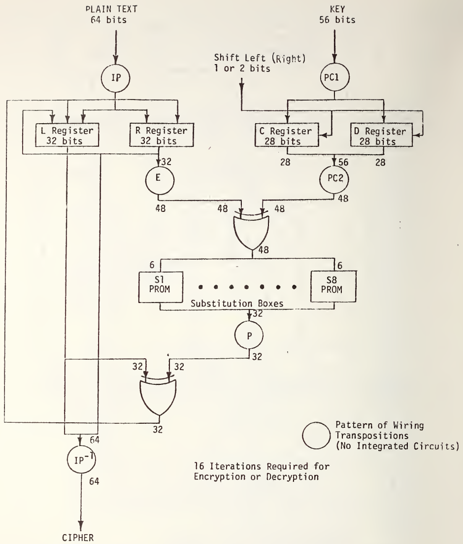
NBS の集積回路版 DES の構成図です。左側では「PLAIN TEXT 64 bits」が円「IP」を経て「L Register 32 bits」「R Register 32 bits」に入ります。右側では「KEY 56 bits」が円「PC1」を経て「C Register 28 bits」「D Register 28 bits」に入り、「Shift Left (Right) 1 or 2 bits」(1 または 2 ビットの左(右)シフト)の入力が両レジスタにかかり、出力(28 と 28、合わせて 56)が円「PC2」に入って 48 ビットを出します。R レジスタの出力(32)は円「E」で 48 ビットになります。2 本の 48 ビット線は排他的論理和のゲートに入り、出力 48 ビットが 6 ビットずつ「S1 PROM」〜「S8 PROM」(「Substitution Boxes」)に分かれ、その 32 ビットの出力が円「P」を経て L レジスタの 32 ビット出力と排他的論理和をとります。結果(32)はレジスタに戻ります。レジスタの 64 ビット出力は円「IP^-1」を経て「CIPHER」になります。凡例は円が「Pattern of Wiring Transpositions (No Integrated Circuits)」(配線による転置のパターン(集積回路なし))を表すことを示し、「16 Iterations Required for Encryption or Decryption」(暗号化・復号に 16 回の繰り返しが必要)と注記があります。
Figure 3. Schematic Diagram of NBS Integrated Circuit Version of DES Encryption Algorithm
図 3. NBS の集積回路版 DES 暗号化アルゴリズムの概略図
3. Summaries of Current and Projected Computer Technology
3. 現在および将来の計算機技術の概要
3.1 Computer Architecture
3.1 計算機アーキテクチャ
An overview of computer architecture was presented by Mr. Jack Lynch, Director of Advanced Development of the Burroughs Corporation. He illustrated the dramatic growth in component density of LSI logic chips using the chart shown in figure 4. At the present time, the CPU for a small business computer could be completely fabricated on a single chip (about 3000 logic gates). According to the projection, one of the largest CPUs could be fabricated on a chip by 1981 (about 250,000 logic gates.) Mr. Lynch pointed out that a logic gate is comprised of several devices, typically about 10. The high-yield chips involved are about 200 by 200 mils, or about 1/2 cm by 1/2 cm. This poses an interesting question for management: what would be the source of corporate income when the largest machine they make can be fitted onto a $10 chip? The answer is felt to lie in the development of comprehensive business systems designed to enable businesses to increase the efficiency of tneir overall operations.
計算機アーキテクチャの概要は、Burroughs Corporation の先端開発ディレクターの Mr. Jack Lynch が発表しました。彼は、LSI 論理チップの部品密度の劇的な増加を、図 4 のグラフで示しました。現在、小型の業務用コンピュータの CPU は、1 つのチップ(約 3,000 論理ゲート)に完全に製作できます。予測によれば、最大級の CPU の 1 つが、1981 年までに 1 つのチップ(約 250,000 論理ゲート)に製作できるようになります。Mr. Lynch は、論理ゲートは複数のデバイス、典型的には約 10 個のデバイスから成ると指摘しました。対象となる高歩留まりのチップは、約 200 ミル × 200 ミル、すなわち約 0.5 cm × 0.5 cm です。これは経営陣にとって興味深い問いを投げかけます。自社が作る最大のマシンが 10 ドルのチップ 1 つに収まるようになったとき、企業の収入源は何になるのでしょうか。その答えは、企業が全体の業務の効率を高められるようにする包括的な業務システムの開発にあると考えられています。
Growth in density of memory chips is illustrated by the chart shown in figure 5. In 1975 the density was about 25,000 bits per chip; it is estimated that this will become about one million bits per chip by 1981. Such densities, while theoretically possible, will require additional research in techniques such as electron-beam lithography in order to be realized.
メモリチップの密度の増加は、図 5 のグラフに示されています。1975 年の密度は 1 チップあたり約 25,000 ビットでしたが、1981 年までには 1 チップあたり約 100 万ビットになると見積もられています。このような密度は、理論的には可能ですが、実現するには電子ビームリソグラフィなどの技術にさらなる研究が必要になります。
Mr. Bigelow asked about the connectivity problem as more components are squeezed onto a chip. Mr. Lynch responded that this did not appear to be an insurmountable problem and offered as evidence the fact that intricate products are currently being fabricated successfully. Mr. Bigelow further asked how many layers of metal could be emplaced for achieving interconnections. This question was answered by Mr. Hillis of Motorola who stated that two layers were generally available in production, but these could be supplemented by using elements as interconnections.
Mr. Bigelow は、チップに詰め込む部品が増えるにつれて生じる接続性の問題について質問しました。Mr. Lynch は、これは克服できない問題とは思われないと答え、その証拠として、現在、込み入った製品が実際にうまく製造されているという事実を挙げました。Mr. Bigelow はさらに、配線を実現するために、金属を何層まで置けるのかを尋ねました。この質問には Motorola の Mr. Hillis が答え、量産では通常 2 層が利用可能ですが、素子を配線として使うことで補える、と述べました。
Initial impetus for LSI development was attributed to the military which provided the resources at first; later on, the commercial and business interests became involved. The comment was made that the volumes required for economic production are becoming so great that potential small users including the Military are being shut out to an increasing degree. Mr. Hillis commented that semiconductor sources are emphasizing low-cost devices, while the drive for higher-speed logic families is losing steam. The commercial thrust is on achieving high density at low cost.
LSI 開発の最初の推進力は軍にあるとされ、軍が最初に資源を提供し、その後、商業や業務の関心が加わりました。経済的な生産に必要な量が非常に大きくなっているため、軍を含む潜在的な小規模の利用者が、ますます締め出されているという指摘がありました。Mr. Hillis は、半導体の供給元は低費用のデバイスを重視しており、より高速な論理ファミリへの意欲は衰えつつあると述べました。商業面の推進力は、低費用で高密度を達成することにあります。
Mr. lynch presented a chart prepared by Booz, Allen & Hamilton showing the distribution of costs incurred by U.S. businesses on information resources, figure 6. Costs for 1975 are shown as $150 billion and are estimated to grow to $350 billion in 1985. From the standpoint of the outside supplier, the greatest potential is in the areas of telecommunications and word processing which greatly outweigh the outlays for EDP. The solution to large-scale business systems, according to Mr. Lynch, involves partitioning the systems into manageable segments. This has three aspects: how to achieve the partitioning, how to implement the segments, and how to create an Operating System which can coordinate the operation of the segments and "avoid chaos". The solution is felt to lie in the use of networks of processors whose operation is properly coordinated. The major unsolved problem is felt to be in the area of software management and the survivability of systems. He conjectured that the necessary techniques might first emerge in dealing with large structured problems such as weather analysis for which large processing arrays were assembled.
Mr. Lynch は、Booz, Allen & Hamilton が作成した、米国企業が情報資源に費やした費用の分布を示すグラフ(図 6)を示しました。1975 年の費用は 1,500 億ドルで、1985 年には 3,500 億ドルに増加すると見積もられています。外部の供給者の立場からは、最大の潜在市場は電気通信とワードプロセッシングの分野であり、EDP への支出をはるかに上回ります。Mr. Lynch によれば、大規模な業務システムの解決策は、システムを扱いやすい部分に分割することにあります。これには 3 つの側面があります。どのように分割するか、各部分をどのように実装するか、そして各部分の動作を調整して「混乱を避ける」ことができるオペレーティングシステムをどのように作るかです。解決策は、動作が適切に調整されたプロセッサのネットワークを使うことにあると考えられています。未解決の主要な問題は、ソフトウェアの管理とシステムの存続性の領域にあると考えられています。彼は、必要な技術は、大規模な処理アレイが組み上げられた気象分析のような、大規模で構造化された問題を扱う中で、最初に現れるかもしれないと推測しました。
As to the role of fiber optics, it was stated that these are being more actively pursued for use in communications, rather than in computers.
光ファイバーの役割については、コンピュータでの利用よりも、通信での利用に向けて、より積極的に追求されていると述べられました。
3.2 Semiconductor Technology
3.2 半導体技術
An overview of semiconductor technology was presented by Mr. Howard Wright of Collins Radio Company. He alluded to the fact that Collins is working on implementations of the DES but placed those efforts outside the scope of his presentation to the Workshop. He expressed the view that density increases of 4 to 1 should not be difficult to achieve. Among the promising new technologies is VLSI (Very Large Scale Integration). He felt that energy density would be kept at present levels by reducing voltages as devices get smaller. Speed increases of about 1.5 megahertz per year have prevailed over about a 10-year period, and he felt that this trend would continue. Speeds of about 30 megahertz, he said, are achievable today. He noted that the speed of a system must be held down to about 1/2 or 1/3 of the maximum speed of the devices, to allow for statistical variations and safe operating margins under worst-case conditions. Power consumption is decreasing; this tends to keep heating problems within bounds, and has also made battery operation more feasible. Complementary Metal-Oxide-Semiconductor (CMOS) circuitry offers very low power levels in the standby mode.
半導体技術の概要は、Collins Radio Company の Mr. Howard Wright が発表しました。彼は、Collins が DES の実装に取り組んでいることに触れましたが、その取組みはワークショップでの自身の発表の範囲外としました。密度を 4 倍にすることは困難ではないはずだという見解を示しました。有望な新技術の中には、VLSI(超大規模集積回路)があります。彼は、デバイスが小さくなるにつれて電圧を下げることで、エネルギー密度は現在の水準に保たれるだろうと考えました。約 10 年にわたって、毎年約 1.5 メガヘルツの速度向上が続いてきており、この傾向は続くだろうと彼は考えました。約 30 メガヘルツの速度は、現在でも達成可能であると述べました。統計的なばらつきや、最悪の場合の条件での安全な動作余裕を見込むため、システムの速度は、デバイスの最大速度の 2 分の 1 または 3 分の 1 程度に抑えなければならないと指摘しました。消費電力は減少しており、これは発熱の問題を抑える傾向があり、バッテリ動作をより実現しやすくもしています。相補型金属酸化膜半導体(CMOS)回路は、待機モードで非常に低い電力水準を実現します。
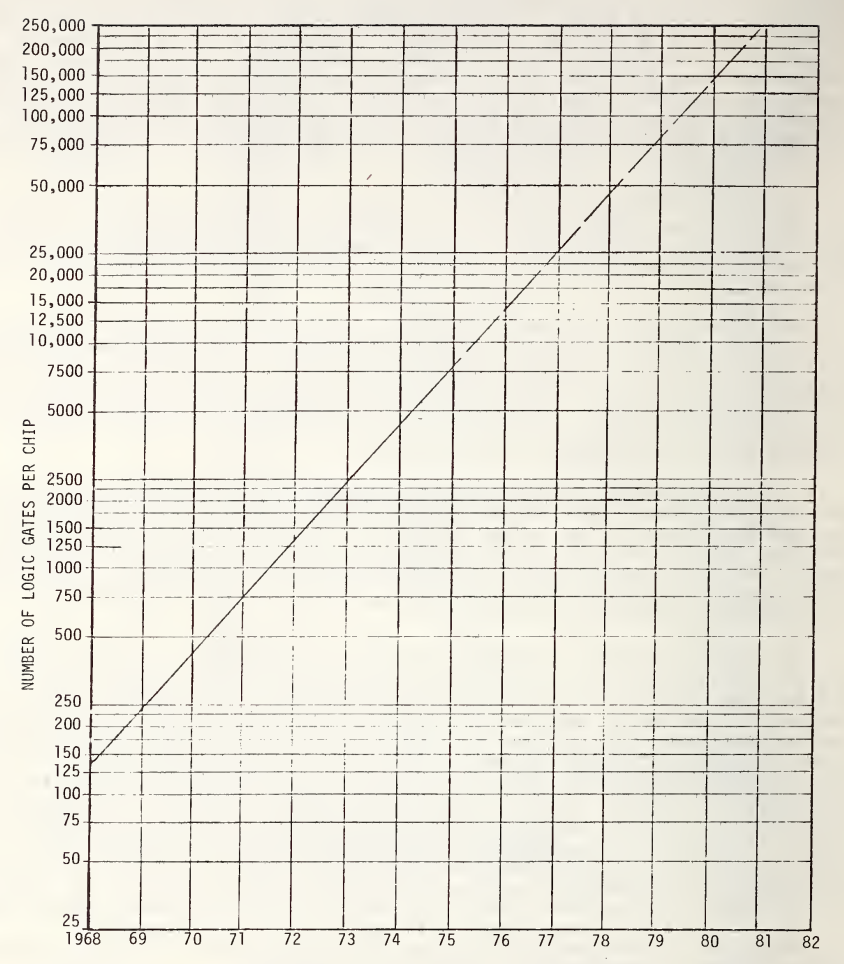
片対数の折れ線グラフです。縦軸は「NUMBER OF LOGIC GATES PER CHIP」(チップあたりの論理ゲート数)で、下端から 25、50、75、100、125、150、200、250、500、750、1000、1250、1500、2000、2500、5000、7500、10,000、12,500、15,000、20,000、25,000、50,000、75,000、100,000、125,000、150,000、200,000、上端の 250,000 まで目盛りがあります。横軸は 1968、69、70、…、81、82 年です。1 本の直線が 1968 年の約 140 から約 1981 年の 250,000 まで上がり、1977 年ごろまでは実線、それ以降は破線です。
FIGURE 4. NUMBER OF LOGIC GATES PER CHIP AS A FUNCTION OF TIME. (CHIP COST IN $10 RANGE FOR MASS-PRODUCED CHIPS.)
図 4. チップあたりの論理ゲート数の経時変化(量産チップのチップ単価が 10 ドル程度の場合)
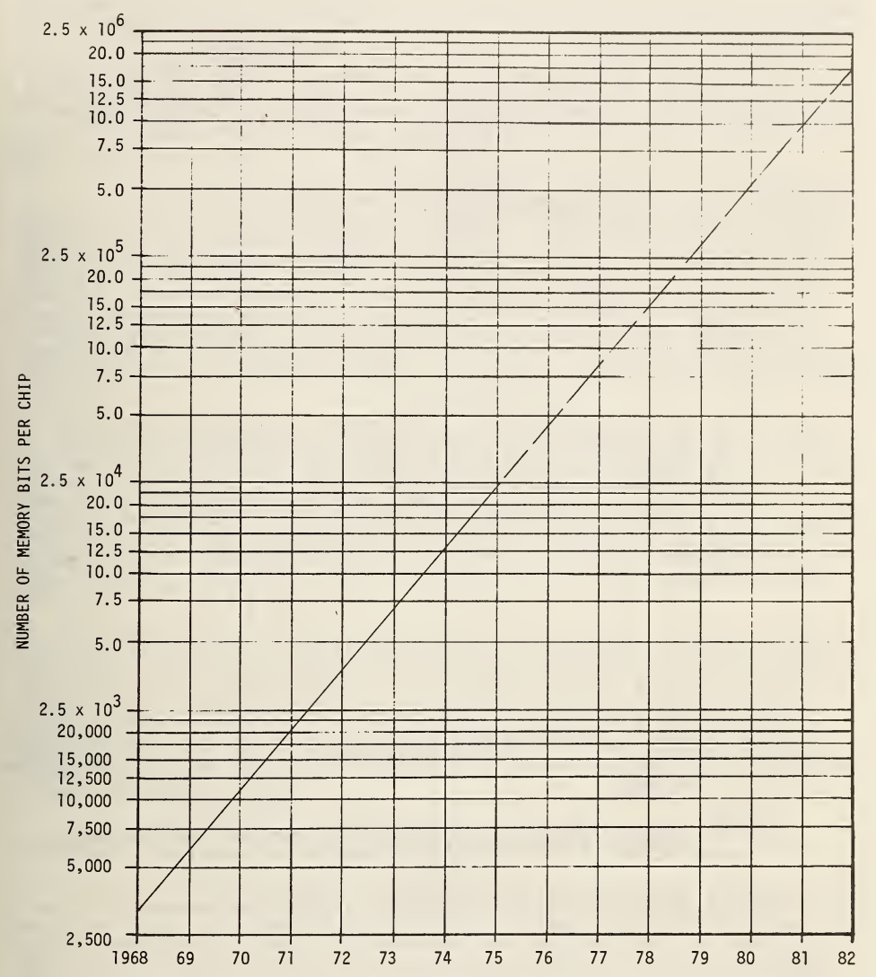
片対数の折れ線グラフです。縦軸は「NUMBER OF MEMORY BITS PER CHIP」(チップあたりのメモリビット数)で、下から 2,500、5,000、7,500、10,000、12,500、15,000、20,000、「2.5 x 10^3」(原文のまま)、5.0、7.5、10.0、12.5、15.0、20.0、「2.5 x 10^4」、5.0、7.5、10.0、12.5、15.0、20.0、「2.5 x 10^5」、5.0、7.5、10.0、12.5、15.0、20.0、上端の「2.5 x 10^6」まで目盛りがあります。横軸は 1968、69、70、…、81、82 年です。1 本の直線が 1968 年の約 3,000 から 1982 年のグラフ上端近くまで上がり、1975 年ごろまでは実線、それ以降は破線です。
Figure 5. Number of Memory Bits per Chip as a Function of Time. (Chip Cost in $10 Range for Mass-Produced Chips.)
図 5. チップあたりのメモリビット数の経時変化(量産チップのチップ単価が 10 ドル程度の場合)
米国の組織による情報資源への支出を 1975 年と 1985 年で比べた図です。凡例(「LEGEND:」)は 4 種のハッチで「EDP」「Telecommunications」(電気通信)「Word Processing and (Paper) Mail」(ワープロと(紙の)郵便)「Travel」(出張)を示します。上の帯は「1975 - $150 Billion」で、区分は 55、3、20、14、26、16、16、中央線の左が「78」、右が「72」です。下の幅広の帯は「1985 - $350 Billion」で、区分は 85、5、40、50、80、65、25、左が「130」、右が「220」です。左に「ACGR 5-6%」、右に「ACGR 11-12%」とあります。下端の横軸は 150 から 0 を経て 250 まで 25 刻みで、0 の左が「PERSONNEL」(人件費)、右が「OUTSIDE SUPPLIERS」(外部供給者)です。 [第三者の画像。第三者の著作物のため、この非公式サイトには掲載していません。原本 PDF を参照してください。]
SOURCES: Booz, Allen & Hamilton, annual reports of major suppliers, FCC reports, Department of Labor (Assuming 5% annual rate of inflation).
出典: Booz, Allen & Hamilton、主要供給者の年次報告書、FCC の報告書、Department of Labor(年率 5% のインフレを想定)。
Figure 6. Expenditures by U. S. Organizations on Information Resources
図 6. 米国の組織による情報資源への支出
Reliability tends to decrease as density goes up, but this is offset by improvements in design. Mr. Wright felt that the emphasis for the Workshop was more properly on maximum performance, rather than maximum density or low power. CMOS circuitry using Silicon-on-Sapphire (SOS) was suggested as probably offering the highest performance if other factors are considered less important. A chart was presented comparing several of the current MOS/LSI processes, figure 7. CMOS-SOS offers a speed of 30 megahertz, which is several times that of the other processes. It has a very low power consumption for its speed, namely a speed-power product of 1 to 2 pico-joules, as compared to 8 to 20 for the other processes. It is presently the most expensive of the current processes, being some 6 times as much as the least expensive process. Mr. Wright pointed out that a new undertaking has associated with it a higher risk factor, and that this further increases the price, at least initially.
信頼性は密度が上がるにつれて低下する傾向がありますが、これは設計の改善によって相殺されます。Mr. Wright は、ワークショップの重点は、最大密度や低消費電力よりも、最大性能に置くほうが適切であると考えました。サファイア上シリコン(SOS)を用いた CMOS 回路は、ほかの要因をあまり重視しないのであれば、おそらく最高の性能を提供するものとして提案されました。現行のいくつかの MOS/LSI プロセスを比較したグラフが示されました(図 7)。CMOS-SOS の速度は 30 メガヘルツで、ほかのプロセスの数倍です。その速度に対して消費電力が非常に低く、速度電力積は 1〜2 ピコジュールで、ほかのプロセスの 8〜20 ピコジュールと比べて小さくなっています。現行のプロセスの中では現時点で最も高価で、最も安価なプロセスの約 6 倍です。Mr. Wright は、新しい事業には、より高いリスク要因が伴い、そのことが少なくとも当初は、価格をさらに押し上げると指摘しました。
Reliability figures were given for various grades of production devices, see figure 8. A military grade chip containing perhaps 500 transistors might be expected to exhibit a reliability of 0.01% failures per 1000 hours, after undergoing a burn-in period. A good grade chip, also burned in, might have a reliability of about 0.03% per 1000 hours. Commercial grade chips, containing 6000 or more transistors, and without burn-in, might be about 0.3% per 1000 hours. These figures refer to hard (permanent) failures. The comment was offered by Mr. Lynch that there may be 20 to 30 soft failures per hard failure. A soft failure may be anything from a momentary transient to a prolonged intermittent condition. For this reason, critical applications should incorporate failure detection and automatic restart provisions.
さまざまな等級の製品デバイスの信頼性の数値が示されました(図 8 を参照)。おそらく 500 個程度のトランジスタを含む軍用グレードのチップは、バーンイン期間を経た後、1,000 時間あたり 0.01% の故障率を示すと見込まれます。同じくバーンインを経た良好なグレードのチップは、1,000 時間あたり約 0.03% の故障率となるでしょう。6,000 個以上のトランジスタを含み、バーンインを行わない民生グレードのチップは、1,000 時間あたり約 0.3% でしょう。これらの数値は、ハード(恒久的)故障を指します。Mr. Lynch は、ハード故障 1 件あたり 20〜30 件のソフト故障があるかもしれないと述べました。ソフト故障は、一瞬の過渡的なものから長引く間欠的な状態まで、さまざまです。このため、重要な用途では、故障の検出と自動再起動の仕組みを組み込むべきです。
In answer to a question by Mr. Bigelow as to how the failure rate varies with time, it was stated that there is a higher infant mortality rate, after which a stable rate prevails. Mr. Hillis noted that the failure rates vary significantly, depending upon the type of circuitry, as for example whether it is dynamic or static, ROMs or RAMs. Dr. Pirtle offered the observation that if ICs were viewed as analog devices rather than digital devices, a great deal more variation would be noted. In practice, digital circuits are exposed to substantial variations arising from a variety of factors. Mr. Hillis observed that while the refresh times for dynamic memory elements theoretically could be in the range of seconds, they were customarily refreshed in milliseconds to achieve a wide margin for reliable operation.
故障率が時間とともにどのように変化するのかという Mr. Bigelow の質問に対し、初期故障率が高く、その後は安定した率になると答えられました。Mr. Hillis は、故障率は、ダイナミックかスタティックか、ROM か RAM かといった回路の種類によって大きく異なると指摘しました。Dr. Pirtle は、IC をデジタルデバイスではなくアナログデバイスとしてみると、はるかに大きなばらつきが認められるだろうと述べました。実際には、デジタル回路はさまざまな要因によって生じる大きなばらつきにさらされています。Mr. Hillis は、ダイナミックメモリ素子のリフレッシュ時間は理論上は秒単位にできるものの、信頼できる動作のために広い余裕をとって、通常はミリ秒単位でリフレッシュされていると述べました。
Semiconductor advancement is currently emphasizing higher density, lower cost, higher speed, lower power, and increased reliability, as illustrated in figure 9.
半導体の進歩は、図 9 に示すように、現在、より高い密度、より低い費用、より高い速度、より低い電力、信頼性の向上を重視しています。
Mr. Bigelow asked what would be considered a good initial quantity to start with for a new item. According to Mr. Wright, this could be 1000 parts if the purchaser would pay all of the start-up costs. Mr. Hillis offered the comment that this could be influenced by the potential to the vendor for additional sales of the same product. In answer to a question by Mr. Lohse on start-up times, it was stated that a new product or a new source for a product would take a period of time, but not as long as was required for the initial effort.
Mr. Bigelow は、新しい品目について、最初の数量としてどのくらいが適切とみなされるかを尋ねました。Mr. Wright によれば、購入者が立上げ費用をすべて負担するなら、1,000 個になりえます。Mr. Hillis は、これは、同じ製品を追加で販売できる可能性という供給者側の事情に左右されうるとの意見を述べました。立上げ時間に関する Mr. Lohse の質問に対しては、新製品や製品の新しい供給元には一定の期間がかかるものの、最初の取組みに必要だった期間ほど長くはかからないと答えられました。
With regard to the achievement of higher densities, Mr. McDonald of Bell Telephone Laboratories stated that various problems might be encountered as wire paths become exceedingly small, one of these being metal migration. He referred to work being done by IBM in this area and referenced a paper by Keyes.*
より高い密度の実現に関して、Bell Telephone Laboratories の Mr. McDonald は、配線経路が極端に小さくなると、金属のマイグレーションなど、さまざまな問題に遭遇する可能性があると述べました。彼は、この分野で IBM が行っている研究に言及し、Keyes の論文を挙げました。*
| PROCESS | Relative Size | Speed MHZ | Relative Complexity to Fabricate | PWR x Delay Pico-Joule | Order of Cost | Maturity Years |
|---|---|---|---|---|---|---|
| P-MOS, METAL GATE, LOW VT, I2 | 1.0 | 1.5 | 1.0 | 20 | 1 | 4 |
| P-MOS, DEPLETION | .62 | 1.5 | 1.2 | 16 | 2 | 3 |
| P-MOS, SILICON GATE, DEPLETION | .43 | 2.0 | 1.4 | 14 | 3 | 2½ |
| N-MOS, Silicon Gate | .45 | 5.0 | 1.4 | 12 | 4 | 3 |
| CMOS BULK | 2.0 | 5.0 | 2.0 | 8 | 4 | 3 |
| CMOS SOS | 1.4 | 30.0 | 1.5 | 1-2 | 6 | 1 |
| I2 L | .45 | 8.0 | 1.5 | 8 | 5 | 1 |
| VLSI (Very Large Scale Integration) | (same) | Same | Same | Same | Large | In development |
| プロセス | 相対的な大きさ | 速度(MHz) | 製造の相対的な複雑さ | 電力 × 遅延(ピコジュール) | 費用の順位 | 成熟までの年数 |
|---|---|---|---|---|---|---|
| P-MOS, METAL GATE, LOW VT, I2 | 1.0 | 1.5 | 1.0 | 20 | 1 | 4 |
| P-MOS, DEPLETION | .62 | 1.5 | 1.2 | 16 | 2 | 3 |
| P-MOS, SILICON GATE, DEPLETION | .43 | 2.0 | 1.4 | 14 | 3 | 2½ |
| N-MOS, Silicon Gate | .45 | 5.0 | 1.4 | 12 | 4 | 3 |
| CMOS BULK | 2.0 | 5.0 | 2.0 | 8 | 4 | 3 |
| CMOS SOS | 1.4 | 30.0 | 1.5 | 1-2 | 6 | 1 |
| I2 L | .45 | 8.0 | 1.5 | 8 | 5 | 1 |
| VLSI(超大規模集積回路) | (同じ) | 同じ | 同じ | 同じ | 大 | 開発中 |
FIGURE 7. COMPARISON OF CURRENT MOS/LSI PROCESSES
図 7. 現行の MOS/LSI プロセスの比較
| FAILURE RATE | |
|---|---|
| MILITARY GRADE | 0.01% / 1000 HRS |
| GOOD GRADE | 0.03% / 1000 HRS |
| COMMERCIAL GRADE | 0.3% / 1000 HRS |
| 故障率 | |
|---|---|
| 軍用グレード | 0.01% / 1,000 時間 |
| 良好なグレード | 0.03% / 1,000 時間 |
| 民生グレード | 0.3% / 1,000 時間 |
FIGURE 8. RELIABILITY LEVELS FOR VARIOUS GRADES OF LSI CHIPS
図 8. さまざまな等級の LSI チップの信頼性水準
•HIGHER DENSITY
•より高い密度
•LOWER COST
•より低い費用
•HIGHER SPEED
•より高い速度
•LOWER POWER
•より低い電力
•INCREASE RELIABILITY
•信頼性の向上
FIGURE 9. DIRECTION OF SEMICONDUCTOR TECHNOLOGY ADVANCEMENT
図 9. 半導体技術の進歩の方向
Regarding density, it was stated that interconnections can cut the density in half, while with silicon there may be a further reduction of 20%.
密度に関しては、相互接続によって密度が半分になりうること、シリコンではさらに 20% 低下する可能性があることが述べられました。
Mr. Hillis directed attention to an article in the February issue of Computer Design, "Trends in Computer Hardware Technology," by David A. Hodges (pp. 77-85), which he felt represented an accurate summary of present and emerging technology. Mr. Hillis particularly noted the dramatic price discontinuity on the chart depicting costs per million instructions per second (MIPS) versus time, in the case of a 3-MIPS microprocessor. This component was displaced below the curve by orders of magnitude, indicating the radical price drop achievable through LSI with high-volume production.
Mr. Hillis は、Computer Design 誌 2 月号の David A. Hodges による記事「Trends in Computer Hardware Technology」(77〜85 ページ)に注意を促し、現在および新たに現れつつある技術の正確な要約になっていると考えました。Mr. Hillis はとくに、100 万命令毎秒(MIPS)あたりの費用の経時変化を示すグラフで、3 MIPS のマイクロプロセッサの場合に価格が劇的に不連続になっている点に注目しました。この部品は、曲線の下に桁違いに外れており、大量生産を伴う LSI によって実現できる大幅な価格の低下を示しています。
4. Technology Aspects of Exhaustive Key Recovery
4. 鍵の全数復元の技術的な側面
4.1 Suggested Design for a Key Extraction Machine
4.1 鍵抽出マシンの設計案
The Workshop was addressed by Mr. Whitfield Diffie of Stanford University who distributed a paper entitled, "Cryptanalysis of the NBS Data Encryption Standard," coauthored by Mr. Diffie and Dr. Martin E. Hellman of the Department of Electrical Engineering, Stanford University. The paper advances the hypothesis that a machine could be built using current technology for extracting keys used with the DES by exhaustion in an average of 10 hours of computation time (20 hours maximum) and that the prorated cost per key extracted would be about $5,000 with a machine whose cost is $20 million. Of greater concern is that the decreasing cost of computation would bring the cost per solution down to perhaps $50 within 10 years. Mr. Diffie stressed that the primary focus of the paper was on the speed and cost of the suggested machine.
Stanford University の Mr. Whitfield Diffie がワークショップで講演し、Mr. Diffie と Stanford University 電気工学部の Dr. Martin E. Hellman の共著による「Cryptanalysis of the NBS Data Encryption Standard」と題する論文を配布しました。この論文は、現在の技術を使って、DES で使われる鍵を全数探索で、平均 10 時間(最大 20 時間)の計算時間で抽出するマシンを製作でき、2,000 万ドルのマシンで、抽出した鍵 1 個あたりの按分費用は約 5,000 ドルになるという仮説を提示しています。さらに懸念されるのは、計算費用の低下により、1 件の解あたりの費用が 10 年以内におそらく 50 ドルまで下がるという点です。Mr. Diffie は、この論文の主な焦点は、提案したマシンの速度と費用にあると強調しました。
Mr. Diffie then reviewed a series of questions which had been posed when they first raised the possibility of building the suggested key extraction machine.
Mr. Diffie は続いて、提案した鍵抽出マシンを製作できる可能性を最初に提起した際に出された、一連の質問を振り返りました。
With regard to the design and control costs for such a machine, Mr. Diffie pointed out that it is not comparable in difficulty to large parallel array-type machines with multiple connections among computing elements. It uses a simple tree structure and each element need only communicate upward to its supervisory element; no sideways paths are involved. Thus, the control problems and design complexity do not escalate with size.
そのようなマシンの設計と制御の費用に関して、Mr. Diffie は、計算要素の間に多数の接続がある大規模な並列アレイ型のマシンとは、難しさが比較にならないと指摘しました。単純な木構造を使い、各要素は上位の監督要素に向けて通信するだけでよく、横方向の経路は関与しません。したがって、制御の問題や設計の複雑さは、規模とともに拡大することはありません。
As to reliability, the computational elements would operate essentially independently, so that continued machine operation is not dependent on all elements working continuously. While the probability of one or more elements failing per day may be high, it is necessary to factor in the probability that the failed element(s) also happen to be assigned the desired key. The joint probability thus becomes exceedingly small. Provision was made in the suggested design for self-testing circuitry and spare components, and allowance was made in the time estimates for diagnostic and repair times. Mr. Bigelow commented that there could be other types of errors, such as the failure to enter the clear text correctly into all of the chips.
信頼性に関しては、計算要素は基本的に独立して動作するため、マシンの継続的な動作は、すべての要素が継続して動作することに依存しません。1 日に 1 個以上の要素が故障する確率は高いかもしれませんが、故障した要素にたまたま求める鍵が割り当てられている確率も考慮する必要があります。そのため、結合確率は非常に小さくなります。提案した設計には、自己試験回路と予備部品の備えが組み込まれ、時間の見積りには診断と修理の時間も見込まれていました。Mr. Bigelow は、すべてのチップに平文を正しく入力できないなど、ほかの種類の誤りもありうると指摘しました。
An objection to the suggested machine was that a single $10 chip could not be used to solve for the key, and that it would take 40 microseconds per key rather than 1 microsecond. As to the required computational speed, Mr. Diffie stated that CMOS-SOS would be capable of meeting this requirement. Mr. Diffie contrasted the design of a chip for their suggested machine with the NBS implementation of the algorithm. In the NBS equipment, most of the time is consumed in I/O operations, while these would be minimal in the suggested machine.
提案されたマシンへの異論として、10 ドルのチップ 1 つでは鍵を解くことはできず、1 つの鍵に 1 マイクロ秒ではなく 40 マイクロ秒かかるだろうというものがありました。必要な計算速度については、Mr. Diffie は、CMOS-SOS ならこの要件を満たせると述べました。Mr. Diffie は、提案したマシンのチップの設計を、NBS のアルゴリズムの実装と対比しました。NBS の機器では、時間の大部分が入出力操作に費やされますが、提案したマシンでは、それは最小限になります。
Mr. Diffie was asked whether he considered it possible to carry out a task of the magnitude involved in building the suggested machine in a clandestine manner. He responded that they were not so concerned with this aspect of the problem; they were more concerned with the fact that, for example, NSA would have the means to carry out such a task through its available channels. Mr. Hillis offered the opinion that RCA would be the only source that could provide such a quantity of SOS chips over a span of a year or two, and that such a capability would be perhaps 4 to 5 years away. Regarding the charts shown in earlier presentations, the comment was made that they apply only to everday applications and do not represent exotic devices (figs. 4 and 5).
Mr. Diffie は、提案したマシンを製作するような規模の作業を、秘密裏に行うことが可能だと考えるか、と尋ねられました。彼は、問題のこの側面はあまり懸念していないと答え、たとえば NSA が、利用可能な経路でそのような作業を実行する手段を持っていることのほうをより懸念していると述べました。Mr. Hillis は、1、2 年の間にこれほどの数の SOS チップを供給できるのは RCA だけであり、そのような能力が整うのはおそらく 4、5 年先だという意見を示しました。先の発表で示されたグラフについては、日常的な用途にのみ適用され、特殊なデバイスを表すものではないという指摘がありました(図 4 と図 5)。
In answer to a question by Mr. Lynch on the number of CMOS-SOS gates that would be needed, Dr. Diffie said that about 5000 would be required. To achieve the fast solution time, a 30 megahertz clock would be required, although there was some conjecture that this speed might have to be doubled.
必要となる CMOS-SOS ゲートの数についての Mr. Lynch の質問に対し、Dr. Diffie は約 5,000 が必要だと答えました。高速な解の算出時間を達成するには、30 メガヘルツのクロックが必要になりますが、この速度は 2 倍にしなければならないかもしれないという推測もありました。
As to the size of the suggested machine, they had used an estimate on the order of 10,000 chips per cabinet, and 1,000,000-chip machine would require 100 cabinets. Power consumption was estimated at 400 kw, which, while large, would not be insurmountable. Mr. Diffie asked the participants whether they might know of comparable-sized machines. Mr. McDonald suggested that itwould be 250 times the size of a large computer memory. Power consumption of the STAR computer was stated to be 250 kw. The Illiac IV was described as occupying 8 cabinets and drawing 250 kw.
提案したマシンの大きさについては、キャビネット 1 台あたり約 10,000 チップという見積りを使っており、1,000,000 チップのマシンには 100 台のキャビネットが必要になります。消費電力は 400 kW と見積もられ、大きいものの、克服できないほどではありません。Mr. Diffie は、同程度の大きさのマシンを知っているかどうか参加者に尋ねました。Mr. McDonald は、大型コンピュータのメモリの 250 倍の大きさになるだろうと述べました。STAR コンピュータの消費電力は 250 kW であると述べられました。Illiac IV は、8 台のキャビネットを占め、250 kW を消費すると説明されました。
Mr. Diffie noted that for purposes of extracting the key, the initial permutations would not be significant, since the transformed version of the key would be the new key for the solution. He suggested the use of read-only memory for the S-boxes. Dr. Pirtle noted that the main source of delay was in the memory references, since all other processing was simply logic gating.
Mr. Diffie は、鍵を抽出するという目的では、初期転置は重要ではないと指摘しました。変換後の鍵が、解を求めるための新しい鍵になるためです。彼は、S ボックスには読み出し専用メモリを使うことを提案しました。Dr. Pirtle は、ほかの処理はすべて単純な論理ゲートによるものであるため、遅延の主な原因はメモリ参照にあると述べました。
Mr. Diffie saw another threat in that at some point in time a machine capable of breaking the algorithm might become available as the result of some legitimate endeavor, such as a large-scale array processor. This might then be diverted to the task of code breaking. While he saw this as unlikely in the next 10 years, he felt that such a machine might certainly become available in less than 25 years and this possibility should be a source of concern.
Mr. Diffie は、もう 1 つの脅威として、ある時点で、大規模アレイプロセッサなど、正当な取組みの結果として、アルゴリズムを破れるマシンが利用可能になるかもしれず、それが暗号解読の作業に転用されるかもしれないと考えました。彼は、今後 10 年以内にはありそうにないと見ていましたが、そのようなマシンは 25 年以内には確実に利用可能になりうると考え、この可能性を懸念すべきだとしました。
Mr. Diffie posed the question as to what might be expected to become available in terms of standard (or slightly modifiable) chips that might be used in a key-extraction machine, or in terms of parallel processors, considering their growth and the research using large arrays of processors.
Mr. Diffie は、プロセッサの増加とプロセッサの大規模アレイを使った研究を考慮して、標準の(またはわずかに改造できる)チップや並列プロセッサの観点から、鍵抽出マシンに使えるものとして何が利用可能になると見込まれるかを問いました。
Mr. Hillis pointed out that there is no such thing as easily producing a slightly modified version of an existing chip. Any modification is equivalent to starting over again.
Mr. Hillis は、既存のチップをわずかに改造した版を容易に製造するようなことは存在しないと指摘しました。どのような改造も、一からやり直すのと同じです。
4.2 Formation of Workshop Subgroups
4.2 ワークショップの小グループの編成
In order to conduct more detailed explorations, the Workshop participants were divided into two subgroups, one on anticipated advances in technology and one on architectures for a key-extraction machine. The subgroup on technology was chaired by Mr. Weiselman and the subgroup on architecture was chaired by Mr. McDonald. These subgroups deliberated for the balance of Monday afternoon and Tuesday morning.
より詳細な検討を行うため、ワークショップの参加者は 2 つの小グループ、すなわち、技術の見込まれる進歩に関するグループと、鍵抽出マシンのアーキテクチャに関するグループに分かれました。技術に関する小グループの議長は Mr. Weiselman が、アーキテクチャに関する小グループの議長は Mr. McDonald が務めました。これらの小グループは、月曜日の午後の残りと火曜日の午前中に審議を行いました。
The Workshop reconvened at 11:00 a.m. on Tuesday, and summaries were presented by the respective subgroup chairmen.
ワークショップは火曜日の午前 11 時に再開され、それぞれの小グループの議長が概要を発表しました。
4.2.1 Summary of Subgroup on Architectures for Key-Extraction Machine
4.2.1 鍵抽出マシンのアーキテクチャに関する小グループの概要
The subgroup summary was presented by Mr. McDonald. Several candidate architectures were offered, together with estimates of cost, speed, development time, and probability of success. These are summarized below:
小グループの概要は、Mr. McDonald が発表しました。費用、速度、開発期間、成功の確率の見積りとともに、いくつかの候補アーキテクチャが示されました。これらを以下に要約します。
•(1) Acquire large-scale, high-speed machine which could be modified for key extraction:
Buy a STAR computer, Est. Cost: $8-10 million, or buy a CRAY 1, Est. Cost $7 million.
Special hardware for functions not readily programmable:
Hardware cost: $400K
Development cost: $400K
System Integration: $1 million, plus 2 years.
Solution rate: 10-40 nanoseconds.
Maximum time to exhaust all possible keys: 23-91 years.
Start 1976, Finish 1978.
•(1) 鍵抽出用に改造できる大規模・高速のマシンを入手する:
STAR コンピュータを購入(見積費用: 800 万〜1,000 万ドル)、または CRAY 1 を購入(見積費用: 700 万ドル)。
容易にプログラムできない機能のための専用ハードウェア:
ハードウェア費用: 40 万ドル
開発費用: 40 万ドル
システム統合: 100 万ドルと 2 年。
解の算出速度: 10〜40 ナノ秒。
可能なすべての鍵を探索し尽くす最大時間: 23〜91 年。
1976 年開始、1978 年完了。
•(2) Acquire future large machine:
Buy "SUPER STAR", Est. Cost $8-10 million.
Build special hardware and add special instructions.
Permutation hardware (2 sets), Functions (2 sets), Special instructions: Est. Cost: $2 million, plus 2 years.
Start 1981, Finish 1982.
•(2) 将来の大型マシンを入手する:
「SUPER STAR」を購入(見積費用 800 万〜1,000 万ドル)。
専用ハードウェアを製作し、専用命令を追加します。
転置ハードウェア(2 組)、関数(2 組)、専用命令: 見積費用 200 万ドルと 2 年。
1981 年開始、1982 年完了。
•(3) Build Pipelined Special Processor:
ECL logic, 20 nanosecond clock, 1000 chips for one solution unit.
Est. development cost: $1 million.
Solution rate: 20 nanoseconds, 50 keys per microsecond.
Exhaustion time for one solution unit: 46 years.
Build machine with 10 solution units:
Exhaustion time: 4.6 years
Est. cost: $1.6 million
Start 1976, Finish 1979.
Build 20 machines:
Exhaustion time: 3 months
Est. cost: $13.5 million
Start 1976, Finish 1982.
Estimated certainty: 60%.
•(3) パイプライン方式の専用プロセッサを製作する:
ECL 論理、20 ナノ秒のクロック、解算出ユニット 1 台あたり 1,000 チップ。
見積開発費用: 100 万ドル。
解の算出速度: 20 ナノ秒、1 マイクロ秒あたり 50 個の鍵。
解算出ユニット 1 台での探索に要する時間: 46 年。
解算出ユニット 10 台のマシンを製作する場合:
探索に要する時間: 4.6 年
見積費用: 160 万ドル
1976 年開始、1979 年完了。
マシン 20 台を製作する場合:
探索に要する時間: 3 か月
見積費用: 1,350 万ドル
1976 年開始、1982 年完了。
見積もられた確実性: 60%。
•(4) Employing exotic technology, e.g., Josephson junction:
50 picosecond clock
Solution rate: 1 nanosecond per solution per substrate.
1000 substrates.
Exhaustion time: 19.8 hours.
Est. cost to develop and fabricate: $50 million.
Start 1985, Finish 1990
Estimated certainty: 10%.
•(4) Josephson 接合など、特殊な技術を採用する:
50 ピコ秒のクロック
解の算出速度: 基板 1 枚あたり、解 1 個につき 1 ナノ秒。
基板 1,000 枚。
探索に要する時間: 19.8 時間。
開発・製作の見積費用: 5,000 万ドル。
1985 年開始、1990 年完了
見積もられた確実性: 10%。
•(5) Million-chip parallel machine:
One million chips:
Est. development cost: $1 million.
Est. cost per chip: $50.
Make and test 104 cards: $20 million.
System development cost: $2 million.
Production: 300 man years.
Size: 64 bays.
Total cost: $72 million.
Power: 3 megawatts; cooling power, 9 Mw., total 12 Mw.
Exhaustion time: 19.8 hours.
Start 1983, Finish 1990
Estimated certainty: 10-20%
•(5) 100 万チップの並列マシン:
100 万チップ:
見積開発費用: 100 万ドル。
チップ 1 個あたりの見積費用: 50 ドル。
104 枚のカードの製作と試験: 2,000 万ドル。
システム開発費用: 200 万ドル。
生産: 300 人年。
規模: 64 ベイ。
総費用: 7,200 万ドル。
電力: 3 メガワット、冷却電力 9 MW、合計 12 MW。
探索に要する時間: 19.8 時間。
1983 年開始、1990 年完了
見積もられた確実性: 10〜20%
•(6) Special low-cost parallel machine (suggested by Mr. McDonald):
Fabricate cards with 70 T2LS chips.
100 cards per bay, 10 bays = 1000 cards.
Solution time per card: 4 microseconds.
Effective solution time for complete machine: 4 nanoseconds per key.
Exhaustion time: 9.14 years.
Est. development cost: $2 million.
Est. total cost: $4 million.
Start 1977, Finish 1979.
Estimated certainty: 70%.
•(6) 専用の低費用並列マシン(Mr. McDonald の提案):
70 個の T2LS チップを搭載したカードを製作します。
1 ベイあたり 100 枚のカード、10 ベイで 1,000 枚のカード。
カード 1 枚あたりの解の算出時間: 4 マイクロ秒。
マシン全体の実効的な解の算出時間: 鍵 1 個あたり 4 ナノ秒。
探索に要する時間: 9.14 年。
見積開発費用: 200 万ドル。
見積総費用: 400 万ドル。
1977 年開始、1979 年完了。
見積もられた確実性: 70%。
(Note: In 1980 - 1982, speed should be ten times as fast.)
(注: 1980〜1982 年には、速度は 10 倍になるはずです。)
Mr. McDonald offered some observations with regard to the above design. He visualized 1000 devices occupying some 10 bays of equipment at a total cost of about one million dollars and having a solution time of 4 microseconds. This would take about 9 years for exhaustion, which would be 4000 times longer than required. But the processing speed/power ratio has been increasing at the rate of about a factor of 10 every 4 years. At this rate, in about 8 years such a machine would have a solution time of about one month. He felt that with a little ingenuity this might rapidly be enhanced.
Mr. McDonald は、上記の設計についていくつかの所見を述べました。彼は、1,000 個のデバイスが約 10 ベイ分の機器を占め、総費用は約 100 万ドル、解の算出時間は 4 マイクロ秒になると想定しました。探索には約 9 年かかり、これは要求される時間の 4,000 倍の長さになります。しかし、処理速度対電力比は、約 4 年ごとに 10 倍の割合で増加しています。この割合なら、約 8 年後には、そのようなマシンの解の算出時間は約 1 か月になるでしょう。少し工夫すれば、これは急速に向上させられるかもしれないと彼は考えました。
The various machine architectures are contrasted in the following chart, figure 10.
さまざまなマシンのアーキテクチャは、次のグラフ(図 10)で対比されています。
4.2.2 Summary of Subgroup on Technology
4.2.2 技術に関する小グループの概要
The subgroup summary was presented by Mr. Wieselman.
小グループの概要は、Mr. Wieselman が発表しました。
Implementation of DES chip using today's technology: NMOS Depletion Load, 50 nanosecond gate delay:
Solution time of 40 microseconds and 160 microseconds for two different manufacturers.
現在の技術による DES チップの実装: NMOS デプレッションロード、ゲート遅延 50 ナノ秒:
2 つの異なる製造者について、解の算出時間は 40 マイクロ秒と 160 マイクロ秒。
Typical cost figures for quantities, based on standard parts, not custom parts assuming about 4 years of production:
NMOS Technology:
0-100K chips per year, $100 per chip;
100K chips per year, $25 per chip;
1 million chips per year, $10 per chip (for 4 years of production).
Confidence level in the above figures is 80%.
数量に応じた典型的な費用の数値。約 4 年の生産を想定し、特注部品ではなく標準部品に基づきます:
NMOS 技術:
年間 0〜10 万チップ、1 チップあたり 100 ドル。
年間 10 万チップ、1 チップあたり 25 ドル。
年間 100 万チップ、1 チップあたり 10 ドル(4 年間の生産の場合)。
上記の数値の信頼水準は 80%。
Future technology, CMOS SOS:
1 microsecond solution time
In quantities of 1 million per year (for 4 years of production):
$50 - 100 per chip for high reliability grade;
$20 per chip for commercial grade.
将来の技術、CMOS SOS:
解の算出時間 1 マイクロ秒
年間 100 万個の数量で(4 年の生産で):
高信頼性グレードで 1 チップあたり 50〜100 ドル。
民生グレードで 1 チップあたり 20 ドル。
Circa 1986:
High speed version: 1/2 microseconds solution time.
Gate delay 1 nanosecond.
3K-30K gates per chip.
3 Watts per chip (practical limit).
0.1 - 1.0 picojoule operating range.
Quantity price $10.
Confidence level in the above figures is 80%.
1986 年頃:
高速版: 解の算出時間 2 分の 1 マイクロ秒。
ゲート遅延 1 ナノ秒。
1 チップあたり 3,000〜30,000 ゲート。
1 チップあたり 3 ワット(実用上の限界)。
動作範囲 0.1〜1.0 ピコジュール。
数量単価 10 ドル。
上記の数値の信頼水準は 80%。
High density version:
Gate delay 10 nanoseconds.
100K gates per chip.
0.1 picojoule
Solution time 1/4 microsecond using pipeline approach.
Quantity price $50 - 100 per chip for high reliability grade;
$10 per chip for commercial grade.
高密度版:
ゲート遅延 10 ナノ秒。
1 チップあたり 100,000 ゲート。
0.1 ピコジュール
パイプライン方式による解の算出時間 4 分の 1 マイクロ秒。
数量単価は、高信頼性グレードで 1 チップあたり 50〜100 ドル、
民生グレードで 1 チップあたり 10 ドル。
Development costs, system costs, and cost of accompanying chips would have to be factored into the above figures.
開発費用、システム費用、付随するチップの費用を上記の数値に織り込む必要があります。
Confidence level in the above figures is 30%.
上記の数値の信頼水準は 30% です。
By 1986, chip sizes would be larger. Greater reliability would be achieved through redundancy. Other technologies such as optics might be expected to appear.
1986 年までに、チップのサイズは大きくなるでしょう。冗長性によって、より高い信頼性が達成されるでしょう。光学など、ほかの技術も登場すると見込まれます。
4.3 General Comments
4.3 全般的な意見
Dr. Pirtle noted that machines with instruction cycles of 20 nanoseconds exist today, and that a solution time of 4 microseconds would be very conservative for a high-speed processor. Some representative arithmetic times were quoted for reference purposes. A floating-point addition for two 32-bit operands was given as 20 nanoseconds. For two 64-bit operands the add time was twice as long, while the multiplication time was four times as long.
Dr. Pirtle は、命令サイクルが 20 ナノ秒のマシンが現在すでに存在しており、高速プロセッサにとって 4 マイクロ秒の解の算出時間は非常に控えめであると指摘しました。参考のため、いくつかの代表的な演算時間が示されました。32 ビットのオペランド 2 つの浮動小数点加算は 20 ナノ秒とされました。64 ビットのオペランド 2 つでは、加算時間は 2 倍、乗算時間は 4 倍の長さでした。
With regard to the number of chips that would be required for a key extraction machine, Mr. Hillis noted that an order for one million chips of a given design would not be considered exceptionally large. Memory chip production is several million per year. The Rockwell calculator chips are being produced at the rate of 2 to 3 million per month. An order for one million chips for a key extraction machine would probably result in a cost closer to $100 than $10. In order to achieve a lower price, one would have to consider a non-American, captive source under control of an adversary. The necessary technology would be a further requirement, and this would take some period of time to achieve.
鍵抽出マシンに必要となるチップの数に関して、Mr. Hillis は、ある設計のチップを 100 万個注文しても、とくに大きな注文とはみなされないと指摘しました。メモリチップは年間数百万個生産されています。Rockwell の電卓用チップは、月に 200 万〜300 万個の割合で生産されています。鍵抽出マシン用にチップを 100 万個注文した場合、費用はおそらく 10 ドルよりも 100 ドルに近くなるでしょう。より低い価格を実現するには、敵対者の支配下にある、米国以外の囲い込まれた供給元を検討する必要があります。必要な技術も別途要件となり、それを実現するには一定の期間がかかります。
Mr. Hillis stated that the life cycle of commercial chips is about 5 years. He pointed out that it takes a production of about 1 million chips to stabilize the yield, and that the price can be reduced 20% for the second million. For a large order, a customer would probably not go to a sole source, and this could double the cost.
Mr. Hillis は、民生用チップのライフサイクルは約 5 年であると述べました。歩留まりを安定させるには約 100 万チップの生産が必要であり、2 回目の 100 万チップでは価格を 20% 下げられると指摘しました。大口の注文の場合、顧客はおそらく単一の供給元には頼まず、それが費用を 2 倍にする可能性があります。
Mr. McDonald wondered whether it might be possible to use arrays of commercial DES chips for building a key extraction machine. He noted, however, that the commercial chips would probably be rather low speed in performance, since they are intended mainly for communications applications, with the data transfer rates being limited by the line speeds. The emphasis in the commercial DES chips will be on moderate speed at low cost.
Mr. McDonald は、市販の DES チップのアレイを使って鍵抽出マシンを製作できないかと考えました。ただし、市販のチップは、おもに通信用途を意図しており、データ転送速度が回線速度で制限されるため、おそらく性能はかなり低速であると指摘しました。市販の DES チップでは、低費用で中程度の速度が重視されることになります。
Mr. Thorpe offered the marketing observation that implementations embodying a component are turning out to add more to the cost of the product than the cost of the component itself.
Mr. Thorpe は、部品を組み込んだ実装によって製品価格に上乗せされる額が、部品自体の価格を上回るようになっているという、市場面の所見を述べました。
The comment was offered that encryption procedures could quickly be changed and this would obsolete a key-extraction machine.
暗号化の手順はすばやく変更でき、そうなれば鍵抽出マシンは陳腐化するという意見が出されました。
5. Computer Security Requirements and the DES
5. コンピュータセキュリティの要件と DES
For the purposes of the Workshop, the DES was selected as a vehicle for exploring significant advances in computer technology, as described in the preceding sections of this report.
ワークショップの目的上、DES は、本報告書の前節までに述べたとおり、計算機技術の重要な進歩を探る媒体として選ばれました。
Numerous comments arose during the Workshop regarding the proposed DES as related to computer security requirements, and these comments are summarized in this section.
ワークショップでは、コンピュータセキュリティの要件に関連して、提案された DES について多くの意見が出ました。それらを本節で要約します。
With regard to the lifetime of the data to be protected by the DES, Mr. Lohse commented that some records would be encrypted for permanent storage, while others would be encrypted only for transmission. Consideration was given to the question of what would constitute a good time frame for the life of the standard. Mr. Secretan of Collins pointed out that the technology is changing too fast to enable projections to be made for more than a few years into the future.
DES で保護されるデータの寿命に関して、Mr. Lohse は、一部の記録は永続的な保存のために暗号化され、ほかの記録は伝送のためだけに暗号化されると述べました。標準の寿命として妥当な期間は何かという問題が検討されました。Collins の Mr. Secretan は、技術の変化が速すぎるため、数年先を超える予測を立てることはできないと指摘しました。
Mr. Maczko of the Incoterm Corporation observed that there seems to be a range of values to be protected, yet the Workshop appeared to be looking at a single solution to protect all values.
Incoterm Corporation の Mr. Maczko は、保護対象となる値には幅があるようですが、ワークショップではすべての値を保護する単一の解決策を検討しているように見えると述べました。
The feeling was expressed among the participants that the DES could be used in various ways to achieve higher levels of security; however, the question was raised as to whether this would fall within the definition of this standard.
参加者の間では、より高い水準のセキュリティを達成するために、DES はさまざまな方法で使えるという認識が示されました。しかし、それがこの標準の定義に含まれるのかどうかという疑問が提起されました。
With regard to the purpose of the Workshop, Mr. Diffie offered the opinion that the interests of the organizers might not correspond to the interests of the participants. He felt it would be helpful to consider what would properly constitute a good standard.
ワークショップの目的に関して、Mr. Diffie は、主催者の関心が参加者の関心と一致していないかもしれないという意見を述べました。彼は、優れた標準とは何かを適切に検討することが有益だと考えました。
| SYSTEM | START | FINISH | COST ($ MILLIONS) | KEY EXHAUSTION TIME | SUCCESS PROBABILITY |
|---|---|---|---|---|---|
| MODIFIED STAR COMPUTER | 1976 | 1978 | 9-11 | 23-91 YRS | -- |
| MODIFIED PROJECTED SUPERCOMPUTER | 1981 | 1982 | 10-12 | 5-12 YRS | 0.6-0.7 |
| PARALLEL MSI | 1977 | 1979 | 4 | 9 YRS | 0.7 |
| PIPELINE ECL | 1976 | 1982 | 13.5 | 3 MONTHS | 0.6 |
| JOSEPHSON JUNCTION | 1985 | 1990 | 50 | 1 DAY | 0.1-0.2 |
| PARALLEL LSI | 1983 | 1990 | 72 | 1 DAY | 0.1-0.2 |
| システム | 開始 | 完了 | 費用(100 万ドル) | 鍵の探索に要する時間 | 成功の確率 |
|---|---|---|---|---|---|
| 改造した STAR コンピュータ | 1976 | 1978 | 9-11 | 23〜91 年 | -- |
| 改造した計画中のスーパーコンピュータ | 1981 | 1982 | 10-12 | 5〜12 年 | 0.6-0.7 |
| 並列 MSI | 1977 | 1979 | 4 | 9 年 | 0.7 |
| パイプライン ECL | 1976 | 1982 | 13.5 | 3 か月 | 0.6 |
| Josephson 接合 | 1985 | 1990 | 50 | 1 日 | 0.1-0.2 |
| 並列 LSI | 1983 | 1990 | 72 | 1 日 | 0.1-0.2 |
Figure 10. Summary of Characteristics of Key Extraction Machines Using Various Architectures
図 10. さまざまなアーキテクチャを用いた鍵抽出マシンの特性の概要
Mr. Bright expressed confidence in the DES as a component, but added that a component by itself isn't an encryption system. He offered the opinion that the standard should be suggestive rather than restrictive for maximum usefulness. He recalled that with the 64-bit key there had originally been discussion over the 8 bits which were not used in the encryption process.
Mr. Bright は、部品としての DES への信頼を表明しましたが、部品それ自体は暗号化システムではないと付け加えました。標準は、最大限の有用性を得るために制限的ではなく示唆的であるべきだという意見を述べました。彼は、64 ビット鍵について、暗号化の過程で使われない 8 ビットをめぐる議論が当初あったことを思い出しました。
Mr. Diffie saw the DES chip as a good component, as far as it goes, but not as a finished product, that is, additional measures should be used to achieve greater security. One technique would be the use of multiple encryption, and he felt that the proposed standard should include such provisions. There was some debate as to how the strength of the algorithm might increase under multiple encryptions. In some systems, encryption under multiple keys is simply equivalent to encryption under some other single key, though this was not felt to be the case with the DES.
Mr. Diffie は、DES チップを、その範囲では優れた部品とみていましたが、完成品とはみていませんでした。つまり、より高いセキュリティを達成するには、追加の対策を使うべきです。1 つの手法は多重暗号化の使用であり、提案された標準にはそのような規定を含めるべきです。多重暗号化によってアルゴリズムの強度がどのように高まりうるかについて、いくらか議論がありました。一部のシステムでは、複数の鍵による暗号化は、単に別の 1 つの鍵による暗号化と等価ですが、DES ではそうではないと考えられました。
Mr. McDonald noted that the existence of a component for performing encryption would strongly influence any actual system. He added that the software people have expressed a desire for "more handles". Mr. James Nelson of Univac expressed the need for an algorithm that was capable of enhancement, but that systems shouldn't be burdened with more than the applications could support.
Mr. McDonald は、暗号化を行う部品が存在することは、実際のどのシステムにも強く影響すると述べました。さらに、ソフトウェア担当者は「より多くの操作手段」を求めていると付け加えました。Univac の Mr. James Nelson は、強化が可能なアルゴリズムが必要ですが、システムにアプリケーションが支えられる以上の負担をかけるべきではないと述べました。
Mr. Lohse cited the SWIFT monetary transfer in which link encryption is used together with end-to-end message authentication. Protection is achieved through key management plus an algorithm plus management of personnel plus the protection of records. There is a need to keep the various aspects in balance. He visualizes a spectrum of protection as being achievable with the DES. It was pointed out that the Gretag equipment used in SWIFT employs a 2000-bit key.
Mr. Lohse は、リンク暗号化とエンドツーエンドのメッセージ認証を併用している SWIFT の資金移動を例に挙げました。保護は、鍵管理、アルゴリズム、要員の管理、記録の保護によって達成されます。さまざまな側面のバランスをとる必要があります。彼は、DES によって、さまざまな段階の保護が達成可能であると思い描いています。SWIFT で使われている Gretag の機器は、2,000 ビットの鍵を使っていることが指摘されました。
In their paper, "Cryptanalysis of the NBS Data Encryption Standard", Dr. Hellman and Mr. Diffie argue that an algorithm having a longer key should be used, in the range of 128 to 256 bits. The paper further argues that a key of this length would not unduly complicate the design of the algorithm nor encumber the user, yet it could increase the security beyond any foreseeable possibility of key extraction by exhaustion. Mr. Diffie was questioned as to how the DES might be expanded to use a key of, say, 112 bits. He pointed out that 768 bits are involved in the 16 rounds which are carried out by the algorithm, and that these iterations would provide an opportunity to introduce additional key bits, rather than depending only on the original 56 bits.
Dr. Hellman と Mr. Diffie は、論文「Cryptanalysis of the NBS Data Encryption Standard」で、128〜256 ビット程度のより長い鍵を持つアルゴリズムを使うべきだと主張しています。この論文はさらに、この長さの鍵なら、アルゴリズムの設計を不当に複雑にすることも、利用者に負担を課すこともなく、全数探索による鍵抽出が予見できるどのような可能性をも超えて、セキュリティを高められると主張しています。Mr. Diffie は、DES を、たとえば 112 ビットの鍵を使うように拡張するにはどうすればよいかを問われました。彼は、アルゴリズムが実行する 16 ラウンドには 768 ビットが関わっており、これらの反復が、元の 56 ビットだけに頼るのではなく、追加の鍵ビットを導入する機会になると指摘しました。
With regard to the use of a longer key, Mr. Diffie pointed out that only about 20% of the gates required to implement the DES are key-dependent. Most of the gates are in the substitution boxes, and these could be implemented with a PROM. There was some debate as to whether the algorithm could be partitioned without requiring excessive pin connections; it would also cost more to implement if it required more than one chip. The Collins representatives noted that the present algorithm is close to the maximum that could be implemented on a chip with present technology; a more complex algorithm might not be realizable for perhaps another two years. Mr. Hillis supported the view that the present key length is about the limit for produceability and that a delay of one to two years might be encountered if a longer key were required.
より長い鍵の使用に関して、Mr. Diffie は、DES の実装に必要なゲートのうち、鍵に依存するのは約 20% にすぎないと指摘しました。ゲートの大半は置換ボックスにあり、これは PROM で実装できます。過剰なピン接続を必要とせずにアルゴリズムを分割できるかどうかについて、いくらか議論がありました。また、複数のチップが必要になれば、実装の費用も増えます。Collins の代表者は、現在のアルゴリズムは、現在の技術で 1 つのチップに実装できる上限に近く、より複雑なアルゴリズムは、おそらくあと 2 年ほど実現できないかもしれないと述べました。Mr. Hillis は、現在の鍵長が製造のしやすさの限界に近く、より長い鍵が必要になれば 1〜2 年の遅れに直面するかもしれないという見解を支持しました。
Mr. Diffie felt that the speed of encryption using a 128-bit key could be comparable to that for the 64-bit key by using more parallelism, but this point was debated. Mr. Bigelow expressed the intuitive feeling that the computation time would necessarily have to be increased for a larger key, in order to realize a more rigorous encryption. He felt that it would not be possible to get adequate mixing by means of parallel processes; at some point it would be necessary to employ serial processes to achieve this.
Mr. Diffie は、128 ビットの鍵を使う暗号化の速度は、並列性を高めることで 64 ビットの鍵の場合に匹敵しうると考えましたが、この点は議論されました。Mr. Bigelow は、より厳密な暗号化を実現するには、より大きな鍵では計算時間を必然的に増やさなければならないだろうという直感を述べました。並列処理だけでは十分な混合を得ることはできず、どこかの時点で、それを達成するために直列処理を使う必要が生じるだろうと彼は考えました。
One way of obtaining greater security with a shorter key is simply to change the key more frequently, but it was pointed out that it is not always convenient to do this. Mr. Hillis wondered whether a satisfactory solution might be to change the key more frequently in proportion to the value of the information being protected. Mr. Diffie called attention to the fact that key generation is fundamental to the encryption process and must be comparably rigorous.
より短い鍵でより高いセキュリティを得る方法の 1 つは、単に鍵をより頻繁に変更することですが、これを行うのは必ずしも便利ではないことが指摘されました。Mr. Hillis は、保護される情報の価値に比例して鍵をより頻繁に変更するのが、満足のいく解決策になるのではないかと考えました。Mr. Diffie は、鍵の生成は暗号化の過程の基礎であり、同程度に厳格でなければならないという点に注意を促しました。
With regard to the utilization of the key bits, it was noted that the DES uses the bits quite uniformly. Each of the 56 bits in the key used by the algorithm is used from 12 to 15 times during the 16 rounds.
鍵ビットの利用に関しては、DES はビットをかなり一様に使っていると指摘されました。アルゴリズムが使う鍵の 56 ビットのそれぞれは、16 ラウンドの間に 12〜15 回使われます。
Mr. Bright noted that the NBS effort is oriented toward hardware. However, he has produced a software version which is available on the NBS 1108. He quoted figures for software execution of the algorithm for a 370/155 and an 1108. These were about 7 milliseconds after the key schedule was generated.
Mr. Bright は、NBS の取組みはハードウェア指向であると指摘しました。しかし、彼はソフトウェア版を作成しており、それは NBS の 1108 で利用可能です。彼は、370/155 と 1108 でのアルゴリズムのソフトウェア実行時間を示しました。鍵スケジュールの生成後、実行時間はいずれも約 7 ミリ秒でした。
Mr. Bright made the observation that the ADP marketplace is seeing for the first time products (i.e., encryption devices employing non-DES algorithms) which are unknown in functions (and dubious, he added). He characterized these as "snake oil" or "unlabelled merchandise" and claimed that with other products from EDP suppliers the customers at least know what they've got. He wondered whether others at the Workshop shared his concern. Mr. Jeffery noted that when a customer purchases a UART* he doesn't ask what is inside. Mr. Bright expressed concern about a product for which the typical customer would have no way to measure the effectiveness of what he was getting.
Mr. Bright は、ADP 市場では初めて、機能が不明な(さらに疑わしい、と彼は付け加えました)製品、すなわち DES 以外のアルゴリズムを使う暗号化装置が見られるようになったと指摘しました。彼は、これらを「いかさま薬」または「ラベルのない商品」と特徴づけ、EDP 供給者のほかの製品なら、顧客は少なくとも何を手に入れたか分かっていると主張しました。彼は、ワークショップの他の参加者も同じ懸念を共有しているかどうかを尋ねました。Mr. Jeffery は、顧客は UART* を購入する際、その中身を尋ねないと指摘しました。Mr. Bright は、一般的な顧客には、手に入れる製品の有効性を測る手段がないことを懸念しました。
Mr. Lohse observed that the DES would be an improvement over the unknown, and often chaotic, situation which is present in the market today.
Mr. Lohse は、DES は、現在の市場にある、未知でしばしば混沌とした状況に比べれば、改善になるだろうと述べました。
6. Concluding Discussion
6. 結びの討論
Upon completion of the summaries presented by the subgroup chairmen, Ed Lohse called upon the Workshop participants for comments. Mr. Bigelow requested that confidence levels be assigned to the projected figures given in the summaries and this was done.
小グループの議長による概要の発表が終わると、Ed Lohse はワークショップの参加者に意見を求めました。Mr. Bigelow は、概要で示された予測の数値に信頼水準を付けるよう求め、それが行われました。
The implications of a single order for 1 million chips were discussed. The cost per chip for such an order was estimated at $50 - $100. It was noted, however, that a supplier probably would not accept a single order for 1 million chips on a one-time basis. Mr. Bigelow asked whether a customer might negoitate on the basis of a larger order, say 5 million chips, then take the first million and disappear. Mr. Hillis pointed out that this was very unlikely, since the supplier would investigate the source of such an order very carefully.
100 万チップの単一の注文が持つ意味が議論されました。そのような注文の 1 チップあたりの費用は、50〜100 ドルと見積もられました。ただし、供給者は、100 万チップの単発注文をおそらく受け入れないだろうと指摘されました。Mr. Bigelow は、顧客がより大きな注文、たとえば 500 万チップを前提に交渉し、最初の 100 万チップを受け取った後で姿を消すことは可能だろうかと尋ねました。Mr. Hillis は、供給者はそのような注文の出どころを非常に注意深く調べるため、これは極めてありそうにないと指摘しました。
Mr. Lohse enquired as to whether everyone was in agreement that the trends put forward in the summaries were factual. He asked if there were any diverging opinions. None were offered.
Mr. Lohse は、概要で示された傾向が事実であることに、全員が同意しているかどうかを尋ねました。彼は、異なる意見があるかどうかを尋ねましたが、出ませんでした。
Mr. Pyke announced to the Workshop that NBS is establishing a validation service for the DES. He solicited the assistance of the participants in helping NBS to verify the correct operation of the test-bed and to determine how it interfaces to the actual equipment that might be brought in. Participants wishing to pursue this further should contact Dr. Branstad.
Mr. Pyke は、NBS が DES の妥当性確認サービスを立ち上げつつあることをワークショップに発表しました。彼は、NBS が試験環境の正しい動作を検証し、持ち込まれうる実際の機器とのインタフェースを判断するのを助けるよう、参加者に協力を求めました。これをさらに進めたい参加者は、Dr. Branstad に連絡してください。
Mr. Jeffery pointed out that the NBS standard refers only to hardware or firmware implementations not changeable by a typical user, as in the case of a microprocessor where the program is contained in a PROM. Mr. Diffie asked whether ROMs would be considered as hardware and Mr. Jeffery responded that these were included in his definition.
Mr. Jeffery は、NBS の標準が指すのは、プログラムが PROM に収められたマイクロプロセッサの場合のように、一般的な利用者が変更できないハードウェアまたはファームウェアによる実装だけであると指摘しました。Mr. Diffie は、ROM はハードウェアとみなされるのかと尋ね、Mr. Jeffery は、それらは自分の定義に含まれると答えました。
The Workshop was concluded with expressions of appreciation to the participants from Dr. Ruth M. Davis, Mr. Lohse, and Mr. Pyke.
ワークショップは、Dr. Ruth M. Davis、Mr. Lohse、Mr. Pyke から参加者への謝意が述べられて、閉会しました。
Appendix A
付録 A
Attendee List
1976 Workshop on Estimation of Significant Advances in Computer Technology
August 30 - 31, 1976
出席者リスト
計算機技術における重要な進歩の推定に関する 1976 年ワークショップ
1976 年 8 月 30〜31 日
[Excerpt from 出席者名簿(個人の氏名・所属), © 各個人(個人情報のため) — not reproduced on this unofficial site]
[出席者名簿(個人の氏名・所属) からの引用。第三者(各個人(個人情報のため))の著作物のため、この非公式サイトには掲載していません。原本 PDF を参照してください。]
APPENDIX B. WORKSHOP BACKGROUND INFORMATION
付録 B. ワークショップの背景情報
1976 WORKSHOP ON ESTIMATION OF SIGNIFICANT ADVANCES IN COMPUTER TECHNOLOGY
計算機技術の重要な進歩の見積りに関する 1976 年ワークショップ
I. PURPOSE
I. 目的
The Institute for Computer Sciences and Technology (ICST) of the National Bureau of Standards has, under Public Law 89-306, certain resoonsibilities for the management of computer technology in the Federal Government. Specifically, it strives to monitor and understand advances in computer sciences and technology, assess their technologically-derived impact and attempt as appropriate to help in their application and acceptance within the Federal Government.
米国標準局(NBS)の計算機科学技術研究所(ICST)は、公法 89-306 に基づき、連邦政府における計算機技術の管理について一定の責任を負っています。具体的には、計算機科学技術の進歩を監視して理解し、技術に由来する影響を評価し、適宜、連邦政府内でのその応用と受け入れを支援しようと努めています。
This Workshop is intended to provide ICST with current scientific and technical information on advances in computer technology which could significantly impact the Federal Government's knowledge and use of computer technology developments in relation to computer security and export administration.
このワークショップは、コンピュータセキュリティと輸出管理に関連して、連邦政府による計算機技術の進展の把握と利用に大きく影響しうる、計算機技術の進歩に関する最新の科学的・技術的情報を ICST に提供することを目的としています。
The focus of the Workshop is to be on advances in the design, architecture and manufacturing of computer systems and related equipment which can be identified or estimated as characterizing the present state-of-the-art and the predictable future.
ワークショップの焦点は、計算機システムと関連機器の設計、アーキテクチャ、製造における進歩で、現在の最新技術水準と予測可能な将来を特徴づけるものとして特定または見積もることができるものに置かれます。
II. SPECIFIC OBJECTIVES
II. 具体的な目標
NBS will use this information to (1) estimate the availability of computer resources necessary to recover the key employed in the NBS-proposed Data Encryption Standard, (2) model advanced computer systems for which computer security safeguards must be emplaced to prevent computer fraud and to meet legislated privacy requirements, and (3) assess the potential technical significance of the proposed export of computer-related products and technology.
NBS は、この情報を、(1) NBS が提案したデータ暗号化標準で使われる鍵を復元するために必要な計算機資源の入手可能性の見積り、(2) コンピュータ詐欺を防ぎ、法制化されたプライバシー要件を満たすためにコンピュータセキュリティの保護対策を講じなければならない高度な計算機システムのモデル化、(3) 計算機関連の製品と技術の輸出案がもつ潜在的な技術的重要性の評価、に使用します。
III. SPECIFIC PROBLEM
III. 具体的な問題
So as to achieve these objectives, the Workshop will address a specific problem as a useful vehicle for examining current and projected capabilities for the design and manufacture of computer systems and related hardware which address specific computational applications. Attention to this particular problem will also be of direct and immediate assistance to NBS in the development of standards and guidelines, especially those related to computer security.
これらの目標を達成するため、ワークショップは、特定の計算の用途に対応する計算機システムと関連ハードウェアの設計・製造における現在および将来の能力を調べる有用な媒体として、具体的な問題を取り上げます。この特定の問題に注意を向けることは、NBS が標準とガイドライン、とくにコンピュータセキュリティに関するものを策定する際にも、直接的かつ即時の助けとなります。
The problem which has been selected is representative of a class of problems whose performance is not assumed to be constrained by traditional computer architectures and techniques. It involves the design and fabrication of a system to perform the algorithm specified in Attachment A. Note that embedded in this algorithm is a function "g", which is the data encryption algorithm recently proposed as a Federal standard by NBS. Attachment B describes this algorithm.
選ばれた問題は、性能が従来の計算機アーキテクチャや技術に制約されるとは想定されない、ある種の問題の代表例です。これは、添付 A に示されたアルゴリズムを実行するシステムの設計と製作に関するものです。このアルゴリズムには、関数「g」が組み込まれており、これは NBS が最近、連邦標準として提案したデータ暗号化アルゴリズムであることに注意してください。添付 B は、このアルゴリズムを説明しています。
IV. QUESTIONS TO BE AOORESSEO
IV. 取り組むべき問題
Among the questions to be considered by the Workshop in addressing this problem are:
この問題に取り組むにあたり、ワークショップが検討する問題には、次のものがあります。
•1. What are the candidate system architectures for implementing this algorithm?
•1. このアルゴリズムを実装するための、候補となるシステムアーキテクチャは何か。
•2. What are the basic performance and cost characteristics of current and projected electronic devices suitable for use in implementations of these architectures, e.g., semiconductor devices, Josephson effect devices, . . .?
•2. これらのアーキテクチャの実装に使うのに適した、現在および将来の電子デバイス(たとえば、半導体デバイス、Josephson 効果デバイスなど)の基本的な性能と費用の特性は何か。
•3. What system designs appear most effective in terms of execution time, error performance, power dissipation, and physical space?
•3. 実行時間、誤り性能、電力損失、物理的な空間の観点から、最も有効と思われるシステム設計はどれか。
•4. What component and system manufacturing limitations may be involved in the implementation?
•4. 実装に関わる可能性のある、部品およびシステムの製造上の制約は何か。
•5. What are the inter-relationships among the basic overall engineering parameters, such as time to successful algorithm execution; cost to design, fabricate, test, operate and maintain; and elapsed time between initiation of design and system operation?
•5. アルゴリズムの実行を成功させるまでの時間、設計・製作・試験・運用・保守の費用、設計の開始からシステムの運用開始までの経過時間といった、基本的な全体の工学的パラメータの間の相互関係は何か。
•6. What is the projected effect on the considerations above of the time of initiation of the effort, e.g., now, twu years from now, five years from now, . . .?
•6. 取組みを開始する時期(たとえば、今、2 年後、5 年後など)が、上記の検討事項に及ぼすと予測される影響は何か。
•7. What additional physical limits or technical resource constraints are applicable?
•7. ほかにどのような物理的限界や技術資源の制約が当てはまりますか。
It is hoped that the answers to these questions will be addressad in quantitative terms and, as applicable, through graphical representations of parametric tradeoffs.
これらの問題への回答は、定量的な形で示され、該当する場合は、パラメータ間のトレードオフをグラフで表現することが期待されます。
V. QUALIFICATIONS OF PARTICIPANTS
V. 参加者の資格
The participants should be recognized experts on capabilities and techniques in one or more of the following areas:
参加者は、次の 1 つ以上の分野における能力と技術について、認められた専門家であるべきです。
•semiconductor manufacturing
•半導体製造
•logic design
•論理設計
•system architecture
•システムアーキテクチャ
•system fabrication
•システム製作
Participants should be able to address the above in terms of the current state-of-the-art as well as near future capabilities and techniques.
参加者は、上記について、現在の最新技術水準および近い将来の能力と技術の観点から論じることができるべきです。
VI. WORKSHOP PROOUCT
VI. ワークショップの成果物
The product of the Workshop will be a technical report on the topics treated, to be produced by NBS (ICST) according to a format to be determined by the Workshop participants. This report will serve as a significant element in NBS' recommendations to the Executive Branch, to Congress, and to public groups for needed actions pertaining to the subject areas of the Workshop.
ワークショップの成果物は、扱った議題に関する技術報告書であり、ワークショップ参加者が決める形式に従って NBS(ICST)が作成します。この報告書は、ワークショップの主題領域に関して必要な対応のために、行政府、議会、公共団体に宛てた NBS の勧告における重要な要素となります。
VII. WORKSHOP ARRANGEMENTS
VII. ワークショップの手配
The Workshop will be held at NBS, Gaithersburg, Maryland on August 30 - 31, 1976 in Dining Room C, Administration Building.
ワークショップは、1976 年 8 月 30〜31 日に、Maryland 州 Gaithersburg の NBS で、管理棟(Administration Building)の食堂 C で開催します。
ATTACHMENT A: EXHAUSTIVE EXTRACTION ALGORITHM
添付 A: 全数抽出アルゴリズム
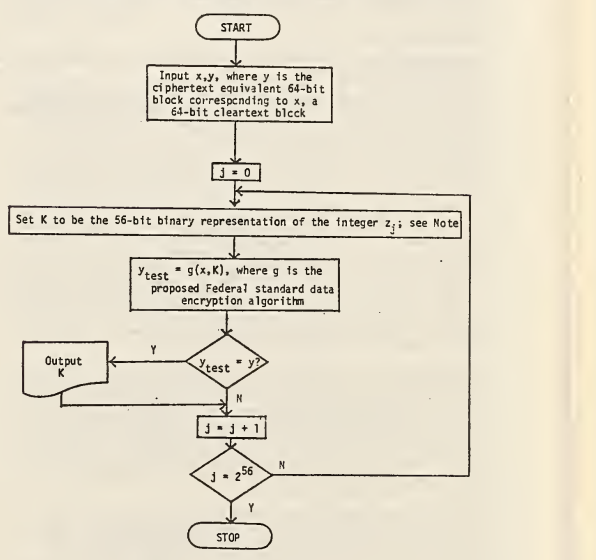
付属書 A の全数抽出アルゴリズムの流れ図です。「START」から「Input x,y, where y is the ciphertext equivalent 64-bit block corresponding to x, a 64-bit cleartext block」(x,y を入力。x は 64 ビットの平文ブロックで、y はそれに対応する暗号文ブロック)、「j = 0」、「Set K to be the 56-bit binary representation of the integer z_j; see Note」(K を整数 z_j の 56 ビットの 2 進表現とする。注を参照)、「y_test = g(x,K), where g is the proposed Federal standard data encryption algorithm」(g は連邦標準として提案されたデータ暗号化アルゴリズム)と進みます。判断「y_test = y?」で「Y」なら左の出力記号「Output K」に進み、その線は判断の下で本流に戻ります。「N」なら下へ進みます。続いて「j = j + 1」、判断「j = 2^56」で、「N」なら右側の線で「Set K」の箱の上に戻り、「Y」なら「STOP」に至ります。
Note:
\(z_j\) may be defined as follows:
let \(z_0 = 0\)
\(z_{j+1} = z_j + 1\)
Any other technique which will systematically generate all keys Kj may in the interval \((0, 2^{56} - 1)\) may be substituted for the above.
注:
\(z_j\) は次のように定義してもよいです。
\(z_0 = 0\) とします
\(z_{j+1} = z_j + 1\)
区間 \((0, 2^{56} - 1)\) のすべての鍵 Kj を系統的に生成する他の手法であれば、上記の代わりに用いてもよいです。
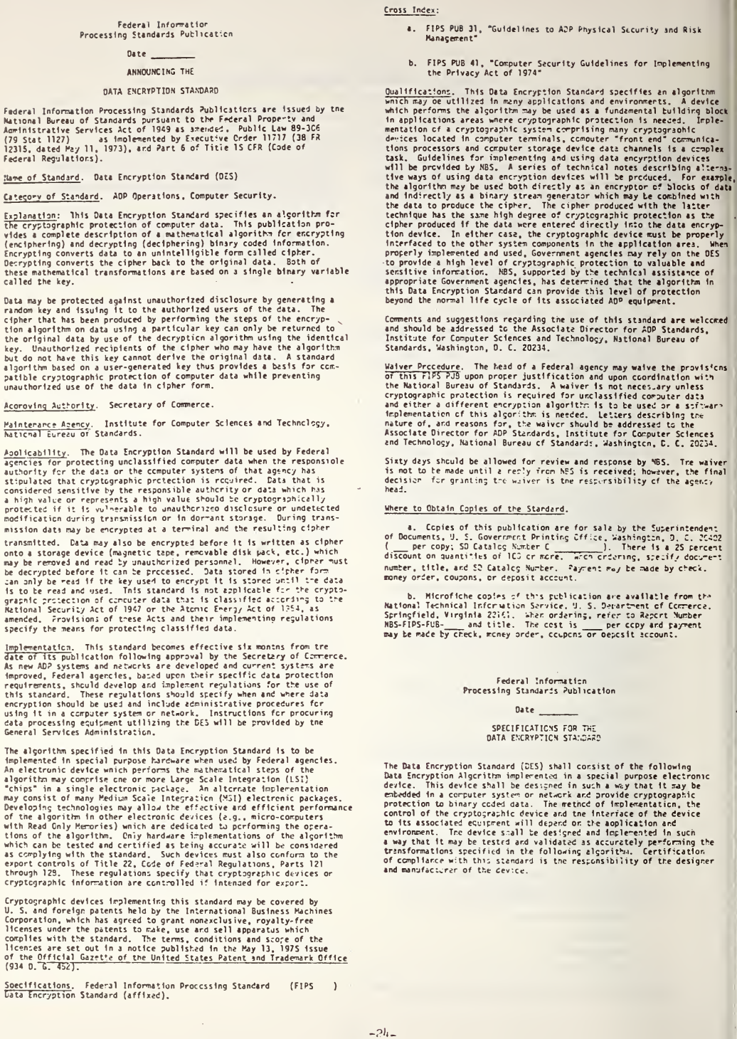
縮小印刷された 2 段組みのページ(-24-)で、データ暗号化規格を告示する連邦情報処理規格刊行物の再録です(刊行物番号と日付は空欄)。左段は「Federal Information Processing Standards Publication」「Date ____」「ANNOUNCING THE」「DATA ENCRYPTION STANDARD」の見出し、FIPS 刊行物の発行に関する前文、下線付きの項目「Name of Standard. Data Encryption Standard (DES)」「Category of Standard. ADP Operations, Computer Security.」「Explanation:」「Approving Authority. Secretary of Commerce.」「Maintenance Agency. Institute for Computer Sciences and Technology, National Bureau of Standards.」「Applicability.」「Implementation.」(ハードウェア実装と IBM の特許・実施許諾の段落が続く)、「Specifications. Federal Information Processing Standard (FIPS ) Data Encryption Standard (affixed).」です。右段は「Cross Index:」(a. FIPS PUB 31「Guidelines to ADP Physical Security and Risk Management」、b. FIPS PUB 41「Computer Security Guidelines for Implementing the Privacy Act of 1974」)、「Qualifications.」、意見募集の段落、「Waiver Procedure.」、「Where to Obtain Copies of the Standard.」(a と b)の後、2 つ目の見出し「Federal Information Processing Standards Publication」「Date ____」「SPECIFICATIONS FOR THE DATA ENCRYPTION STANDARD」とその冒頭の段落です。
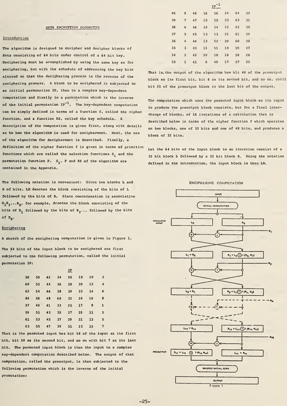
縮小印刷された 2 段組みのページ(-25-)で、「DATA ENCRYPTION ALGORITHM」(データ暗号化アルゴリズム)の冒頭の再録です。左段は見出し「DATA ENCRYPTION ALGORITHM」、節「Introduction」、ブロックの連結の記法の段落、節「Enciphering」(「A sketch of the enciphering computation is given in Figure 1.」)、表「IP」(初期転置、8 行 8 列のビット番号)とその説明です。右段は表「IP^-1」(逆初期転置、8 行 8 列)とその説明、暗号関数 f の 16 回の繰り返しと入力ブロック LR に関する段落、図「ENCIPHERING COMPUTATION」(「Figure 1」)です。図は「INPUT」「INITIAL PERMUTATION」から「PERMUTED INPUT」を L0 と R0 に分け、鍵 K1、K2、…、K16 と f による段で「L1 = R0」「R1 = L0 ⊕ f(R0, K1)」から「L15 = R14」「R15 = L14 ⊕ f(R14, K15)」までを求め、「PREOUTPUT」(「R16 = L15 ⊕ f(R15, K16)」「L16 = R15」)、「INVERSE INITIAL PERM」「OUTPUT」に至ります。
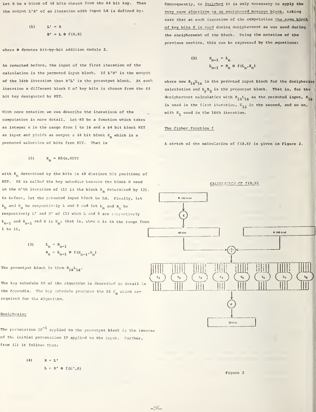
縮小印刷された 2 段組みのページ(-26-)で、「DATA ENCRYPTION ALGORITHM」の続きの再録です。左段は 1 回の繰り返しの定義、式 (1)「L' = R」「R' = L ⊕ f(R,K)」、鍵スケジュール KS を定める式 (2)「K_n = KS(n,KEY)」、式 (3)「L_n = R_n-1」「R_n = L_n-1 ⊕ f(R_n-1,K_n)」と、節「Deciphering」(復号)の式 (4)「R = L'」「L = R' ⊕ f(L',K)」です。右段は復号の式 (5)「R_n-1 = L_n」「L_n-1 = R_n ⊕ f(L_n,K_n)」、節「The Cipher Function f」(「A sketch of the calculation of f(R,K) is given in Figure 2.」)、図「CALCULATION OF f(R,K)」(「Figure 2」)です。図は「R (32 bits)」が「E」で「48 bits」になり「K (48 bits)」と加算され、結果が選択関数 S1〜S8 に分かれ、その出力が「P」を経て「32 bits」になることを示します。
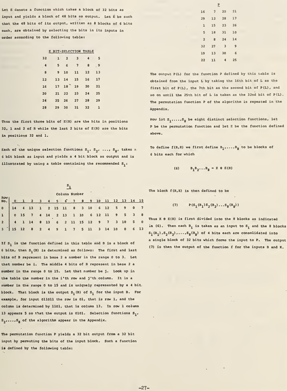
縮小印刷された 2 段組みのページ(-27-)で、「DATA ENCRYPTION ALGORITHM」の続きの再録です。左段は関数 E の定義と表「E BIT-SELECTION TABLE」(E ビット選択表、8 行 6 列)、選択関数 S1、…、S8 の説明と表「S1」(横に「Column Number」0〜15、縦に「Row No.」0〜3)、S1(B) の引き方とその例、転置関数 P の導入です。右段は表「P」(8 行 4 列)とその説明、式 (6)「B1B2...B8 = K ⊕ E(R)」と式 (7)「P(S1(B1)S2(B2)...S8(B8))」による f(R,K) の定義です。
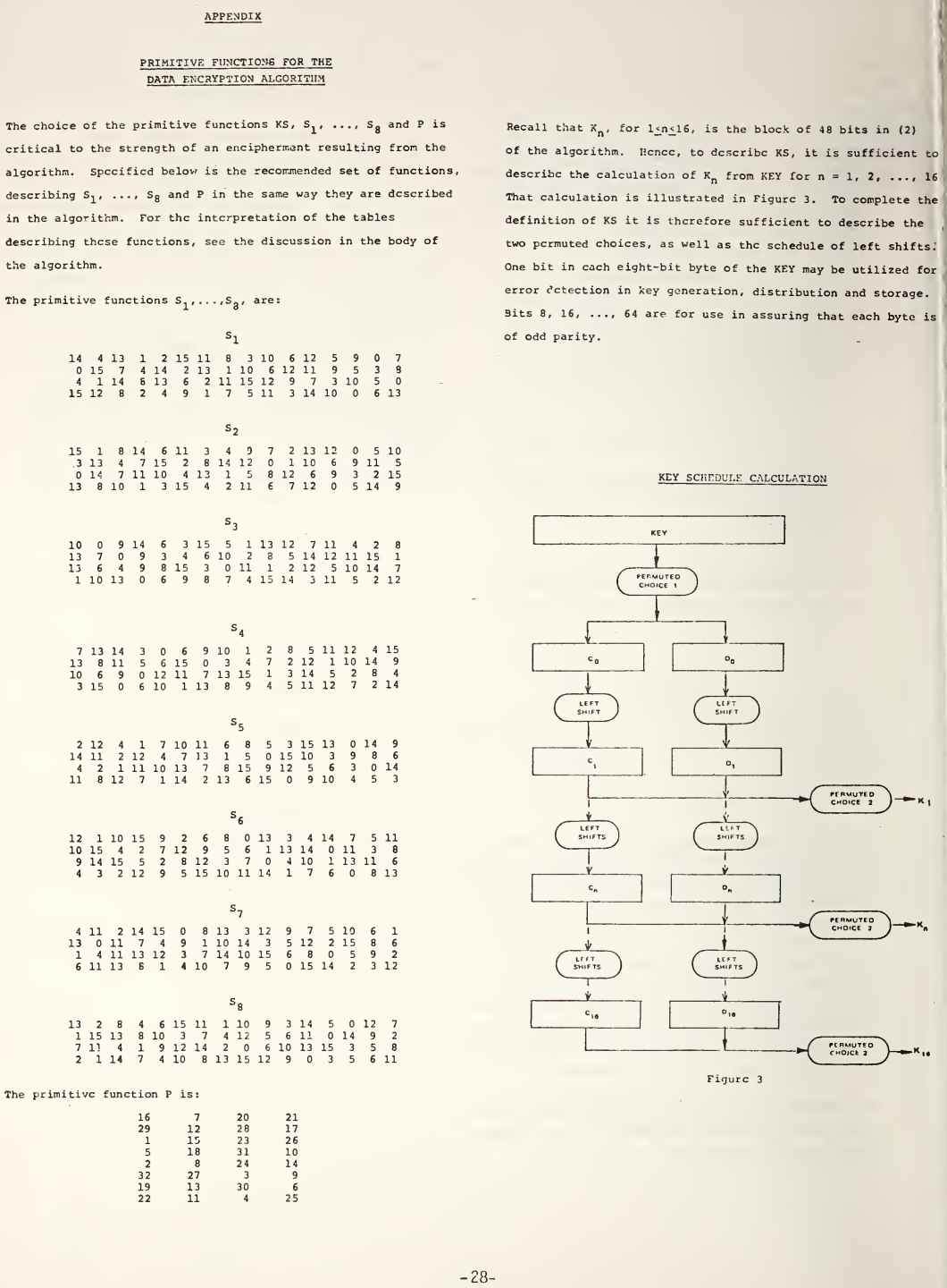
縮小印刷された 2 段組みのページ(-28-)で、アルゴリズムの付録の再録です。左段は見出し「APPENDIX」「PRIMITIVE FUNCTIONS FOR THE DATA ENCRYPTION ALGORITHM」(データ暗号化アルゴリズムの基本関数)、前文、「The primitive functions S1,...,S8, are:」に続く 8 つの表「S1」〜「S8」(各 4 行 16 列)、「The primitive function P is:」と P の表です。右段は KEY から K_n を求める計算による KS の記述、2 つの転置選択と左シフト回数のスケジュール、パリティ用のビット 8、16、…、64 に関する段落と、図「KEY SCHEDULE CALCULATION」(鍵スケジュールの計算、「Figure 3」)です。図は「KEY」が「PERMUTED CHOICE 1」で C0 と D0 に分かれ、「LEFT SHIFT」「LEFT SHIFTS」で C1、D1、…、Cn、Dn、…、C16、D16 を得て、各段で「PERMUTED CHOICE 2」が K1、…、Kn、…、K16 を出すことを示します。
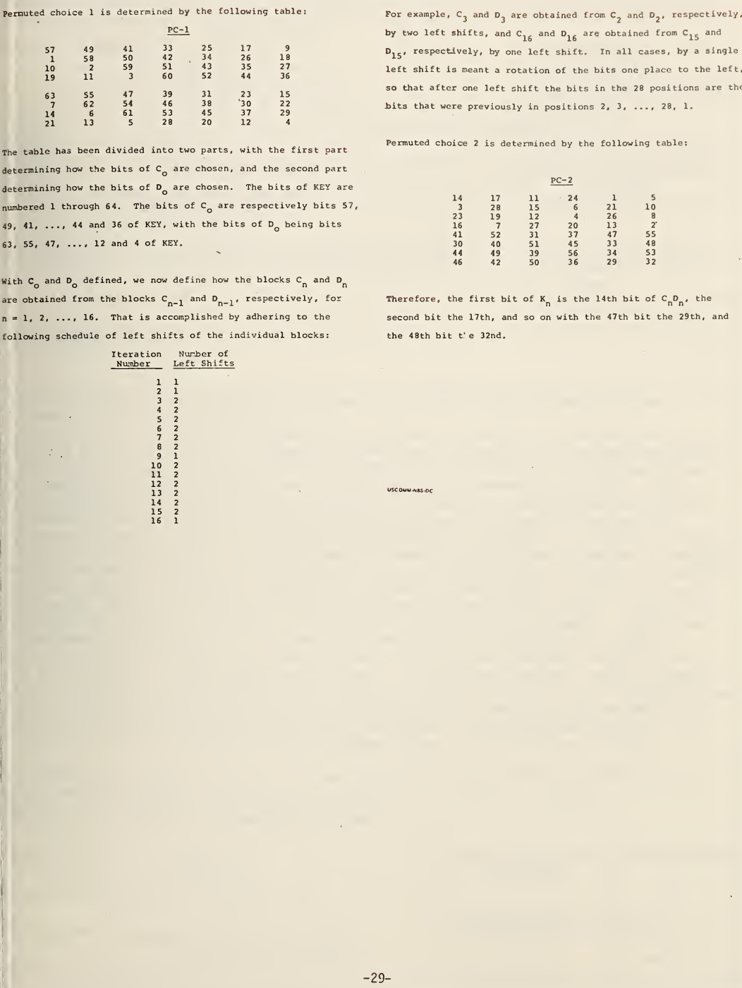
縮小印刷された 2 段組みのページ(-29-)で、アルゴリズムの付録の終わりの再録です。左段は「Permuted choice 1 is determined by the following table:」と表「PC-1」(C0 用と D0 用の 2 部分、各 4 行 7 列)、その説明、「Iteration Number」(1〜16)と「Number of Left Shifts」の 2 列からなる左シフトの予定表です。右段は左シフトで C と D を得る例と 1 回の左シフトの定義、「Permuted choice 2 is determined by the following table:」と表「PC-2」(8 行 6 列)、その説明です。右段の下に小さく「USCOMM-NBS-DC」の印刷所の記号があり、ページの残りは空白です。
| NBS-114A (REV. 7-73) | |
| U.S. DEPT. OF COMM. BIBLIOGRAPHIC DATA SHEET | |
| 1. PUBLICATION OR REPORT NO. | NBSIR 76-1189 |
| 2. Gov't Accession No. | |
| 3. Recipient's Accession No. | |
| 4. TITLE AND SUBTITLE | Report of the 1976 Workshop on Estimation of Significant Advances in Computer Technology |
| 5. Publication Date | December 1976 |
| 6. Performing Organization Code | |
| 7. AUTHOR(S) | Paul Meissner |
| 8. Performing Organ. Report No. | |
| 9. PERFORMING ORGANIZATION NAME AND ADDRESS | NATIONAL BUREAU OF STANDARDS DEPARTMENT OF COMMERCE WASHINGTON, D.C. 20234 |
| 10. Project/Task/Work Unit No. | 6501115 |
| 11. Contract/Grant No. | |
| 12. Sponsoring Organization Name and Complete Address (Street, City, State, ZIP) | Same as item 9. |
| 13. Type of Report & Period Covered | Final |
| 14. Sponsoring Agency Code | |
| 15. SUPPLEMENTARY NOTES | |
| 16. ABSTRACT (A 200-word or less factual summary of most significant information. If document includes a significant bibliography or literature survey, mention it here.) | A workshop on the estimation of significant advances in computer technology was conducted by the Institute for Computer Sciences and Technology at the National Bureau of Standards on August 30-31, 1976. The workshop was attended by 20 representatives from industry, research organizations, universities and Government agencies. The workshop was held to obtain current scientific and technical information on advances in computer technology which could significantly impact the Federal Government's knowledge and use of computer technology developments in relation to computer security and export administration. Presentations were made on anticipated advances in computer architecture and semiconductor technology. It was indicated that the present trends in component density for LSI will continue to increase at the current rate for at least five years. The speed of logic circuitry has been increasing at a rate of about 1.5 megaHertz per year, and a speed of 30 megahertz is presently attainable. Speed-power ratios have been improving by a factor of 10 about every 4 years, and a similar improvement appears likely in the next 4 years. The current emphasis in development work is on achieving high density at low cost. In order to provide a vehicle around which to organize its discussions, the workshop considered the design of a hypothetical machine for extracting the key used for encrypting data under the proposed NBS Data Encryption Standard. Several designs were postulated and engineering estimates were developed for operating speed, size, development time, cost, and other factors. |
| 17. KEY WORDS (six to twelve entries; alphabetical order; capitalize only the first letter of the first key word unless a proper name; separated by semicolons) | Computer architecture; computer security; computer technology; encryption; semiconductor technology; technology advances |
| 18. AVAILABILITY | [X] Unlimited [ ] For Official Distribution. Do Not Release to NTIS [ ] Order From Sup. of Doc., U.S. Government Printing Office Washington, D.C. 20402, SD Cat. No. C13 [X] Order From National Technical Information Service (NTIS) Springfield, Virginia 22151 |
| 19. SECURITY CLASS (THIS REPORT) | UNCLASSIFIED |
| 20. SECURITY CLASS (THIS PAGE) | UNCLASSIFIED |
| 21. NO. OF PAGES | 33 |
| 22. Price | $4.00 |
| NBS-114A(REV. 7-73) | |
| 米国商務省 書誌データシート | |
| 1. 刊行物または報告書番号 | NBSIR 76-1189 |
| 2. 政府受入番号 | |
| 3. 受領者の受入番号 | |
| 4. 題名および副題 | 計算機技術の重要な進歩の見積りに関する 1976 年ワークショップの報告書 |
| 5. 発行日 | 1976 年 12 月 |
| 6. 実施組織コード | |
| 7. 著者 | Paul Meissner |
| 8. 実施組織の報告書番号 | |
| 9. 実施組織の名称および住所 | 米国標準局(NATIONAL BUREAU OF STANDARDS) 米国商務省(DEPARTMENT OF COMMERCE) WASHINGTON, D.C. 20234 |
| 10. プロジェクト/タスク/作業単位番号 | 6501115 |
| 11. 契約/助成番号 | |
| 12. 後援組織の名称および完全な住所(番地、市、州、郵便番号) | 項目 9 と同じ。 |
| 13. 報告書の種類および対象期間 | 最終 |
| 14. 後援機関コード | |
| 15. 補足注記 | |
| 16. 要旨(最も重要な情報の 200 語以内の事実に基づく要約。文書に重要な参考文献一覧や文献調査が含まれる場合は、ここに記載します。) | 米国標準局(NBS)の計算機科学技術研究所(ICST)は、1976 年 8 月 30〜31 日に、計算機技術の重要な進歩の見積りに関するワークショップを実施しました。ワークショップには、産業界、研究機関、大学、政府機関から 20 人の代表者が出席しました。このワークショップは、コンピュータセキュリティと輸出管理に関連して、連邦政府による計算機技術の進展の把握と利用に大きく影響しうる、計算機技術の進歩に関する最新の科学的・技術的情報を得るために開催されました。計算機アーキテクチャと半導体技術について、見込まれる進歩に関する発表が行われました。LSI の部品密度の現在の傾向は、少なくとも 5 年間は現在の割合で増加し続けると示されました。論理回路の速度は毎年約 1.5 メガヘルツの割合で向上しており、現在は 30 メガヘルツの速度が達成可能です。速度対電力比は約 4 年ごとに 10 倍ずつ改善されており、今後 4 年間も同様の改善が見込まれます。開発作業における現在の重点は、低費用で高密度を達成することにあります。議論を組み立てる媒体とするため、ワークショップは、提案された NBS データ暗号化標準でデータを暗号化する際に使われる鍵を抽出する仮想のマシンの設計を検討しました。いくつかの設計が想定され、動作速度、規模、開発期間、費用、その他の要因について、工学的な見積りが作成されました。 |
| 17. キーワード(6〜12 項目。アルファベット順。固有名詞でない限り、最初のキーワードの頭文字のみ大文字。セミコロンで区切る) | 暗号化、計算機アーキテクチャ、計算機技術、コンピュータセキュリティ、半導体技術、技術の進歩 |
| 18. 入手方法 | [X] 無制限 [ ] 公式配布用。NTIS には提供しない [ ] Sup. of Doc., U.S. Government Printing Office Washington, D.C. 20402, SD Cat. No. C13 から注文 [X] National Technical Information Service (NTIS) Springfield, Virginia 22151 から注文 |
| 19. 機密区分(本報告書) | 非機密 |
| 20. 機密区分(本ページ) | 非機密 |
| 21. ページ数 | 33 |
| 22. 価格 | $4.00 |